Touch panel substrate

a technology of touch panel substrate and substrate, applied in the field of touch panel substrate, can solve the problems of electrostatic breakdown, touch controller may be led, electrostatic breakdown, etc., and achieve the effect of preventing a detection circuit from being broken down

Inactive Publication Date: 2016-04-07
SHARP KK
View PDF29 Cites 18 Cited by
  • Summary
  • Abstract
  • Description
  • Claims
  • Application Information

AI Technical Summary

Benefits of technology

[0018]According to an aspect of the present invention, it is possible to provide a touch panel substrate which can prevent a detection circuit from being broken down due to voltage application of static electricity, by blocking static electricity into a sensor electrode formation surface of a substrate.

Problems solved by technology

Such an electrostatic capacitive touch panel substrate has a problem in that, in a case where an external electrostatic voltage is applied to the sensor electrodes, the electrostatic capacitive touch panel substrate may malfunction or the touch controller may be led to electrostatic breakdown.

Method used


Image

  • Touch panel substrate
  • Touch panel substrate
  • Touch panel substrate

Examples


embodiment 1

[0035]The following discusses an embodiment of the present invention in detail with reference to FIGS. 1 through 6.

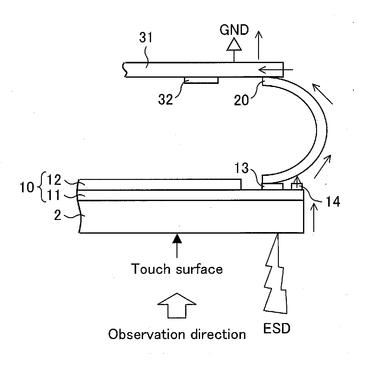
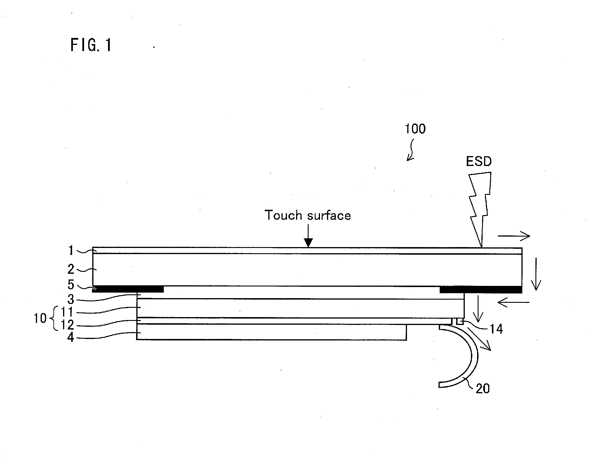
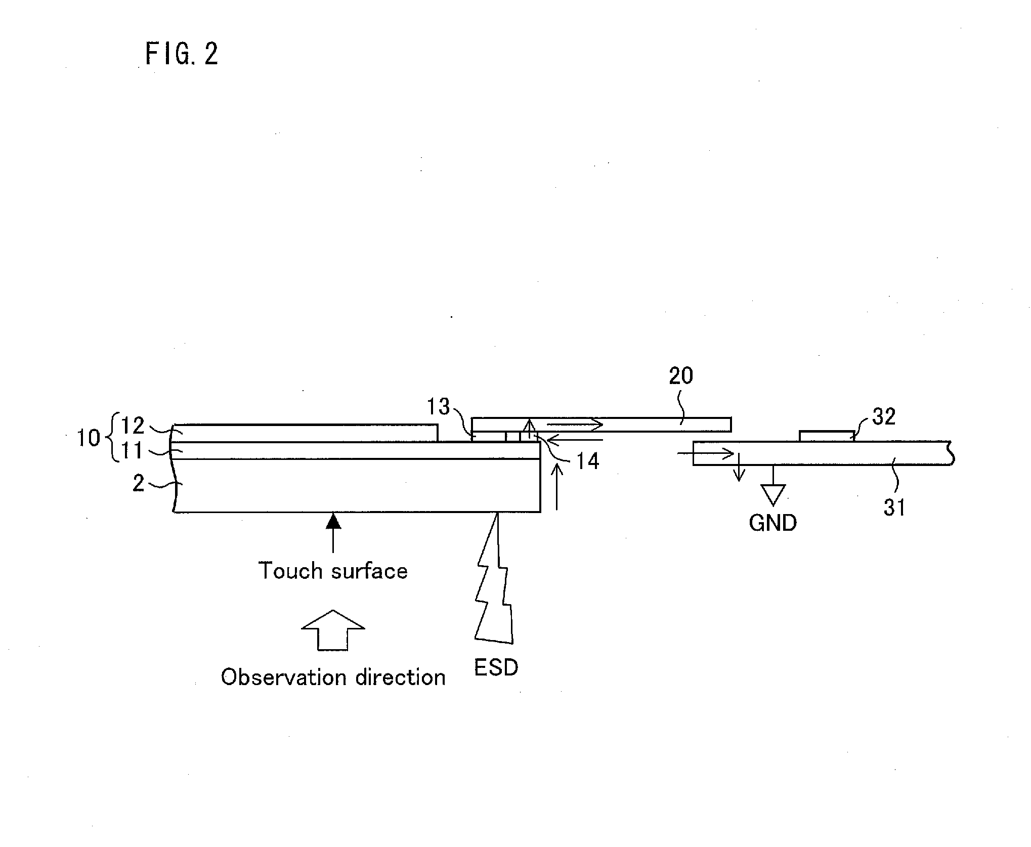
[0036]FIG. 1 is a cross-sectional view of a touch panel substrate of Embodiment 1. FIG. 2 is a cross-sectional view illustrating a connection relation between a first electrode substrate and a touch controller in the touch panel substrate of Embodiment 1. FIG. 3 is a cross-sectional view illustrating a connection relation between the first electrode substrate and the touch controller in a case where a flexible substrate is bent.

[0037]As illustrated in FIG. 1, a touch panel substrate 100 is configured to include an AR (Anti Refrection) film 1 for preventing reflection of external light, a cover glass 2, an OCA (Optical Clear Adhesive, transparent optical adhesive film) 3, a first electrode substrate 10 provided with sensor electrodes, and a protective substrate 4, which are laminated in this order.

[0038]In the touch panel substrate 100, a surface of the AR film 1 constit...

example 1

[0050]FIG. 4 is a plan view illustrating a back surface side of a first electrode substrate in accordance with an example of Embodiment 1.

[0051]As illustrated in FIG. 4, a back surface of a first substrate 11 is provided with a sensor active area 15 in which a plurality of sensor electrodes is formed. The plurality of sensor electrodes provided in the sensor active area 15 includes a plurality of first sensor electrodes formed so as to extend in a first direction and a plurality of second sensor electrodes formed to extend in a second direction orthogonal to the first direction, which first sensor electrodes and the second sensor electrodes are not illustrated in FIG. 4.

[0052]The first substrate 11 is provided, outside the sensor active area 15, a wiring area 16A for collecting lines which are connected to the first sensor electrodes, respectively, and a wiring area 16B for collecting lines which are connected to the second sensor electrodes, respectively.

[0053]Outside the wiring ar...

example 2

[0067]The following discusses other examples of Embodiment 1, with reference to FIGS. 7 through 11. Note that, for convenience of explanation, members having functions identical to those of respective members described in the above Examples are given identical reference signs, respectively, and descriptions thereof are omitted here.

[0068]FIG. 7 is a plan view illustrating a back surface of a first electrode substrate in accordance with another example of Embodiment 1.

[0069]A first electrode substrate 10 in accordance with Example 2 is provided with two GND terminals 18C as a result of connection of a flexible substrate to a back surface of a first substrate 11. Here, the two GND terminals 18C are provided so as to sandwich a terminal section 13A, as illustrated in FIG. 7.

[0070]The GND terminals 18C of the present embodiment are shorter than the GND terminals 18A of Example 1. The GND terminals 18C are provided so as to sandwich only an end portion of the terminal section 13A. In thi...


PUM


Abstract

The present invention provides a touch panel substrate capable of preventing a detection circuit from being broken down due to application of electrostatic voltage. The touch panel substrate includes a flexible substrate (20) for electrically connecting sensor electrodes (12) and a touch controller (32) to each other. The flexible electrode (20) has one end connected to a terminal section (13) including terminals. The touch panel substrate is further provided with a shielding electrode (14), on an outer side of the terminal section (13).

Description

TECHNICAL FIELD [0001]The present invention relates to a touch panel substrate.BACKGROUND ART [0002]Recently, widely used as portable telephone devices, laptops, and the like are electronic devices provided with a touch panel substrate which can detect a position of a detection target object in a case where a finger or a pen for input (detection target object) touches or approaches a display surface of a display device. The touch panel substrate is provided on the display surface of the display device in such electronic devices.[0003]For example, an electrostatic capacitive touch panel substrate includes: (a) an electrode layer in which a plurality of first sensor electrodes extending in a first direction and second sensor electrodes extending in a second direction orthogonal to the first direction are formed; and (b) a touch controller for calculating a position of a detection target object on the basis of a change in electrostatic capacitance which is formed between the first sens...

Claims


Application Information

Patent Timeline
Patent Type & Authority Applications(United States)
IPC IPC(8): G06F3/041G06F3/047G06F3/044
CPCG06F3/0416G06F3/044G06F2203/04107G06F3/047G06F2203/04102G06F3/0412G06F3/04164H05K9/0067G06F3/041
Inventor KIDA, KAZUTOSHIMIYAMOTO, MASAYUKIITOH, MOTOMITSUYOSHIMURA, KAZUYA
Owner SHARP KK
Why Eureka
Try Eureka