Touch control liquid crystal display device

Active Publication Date: 2014-06-19
SHANGHAI TIANMA MICRO ELECTRONICS CO LTD
View PDF3 Cites 61 Cited by
  • Summary
  • Abstract
  • Description
  • Claims
  • Application Information

AI Technical Summary

Benefits of technology

[0011]One inventive aspect is a touch control liquid crystal display device. The liquid crystal display device includes a color film substrate, a thin film transistor array substrate, and a liquid crystal layer arranged between the color film substrate and the thin film transistor array substrate. The color film substrate includes a grid-shaped black matrix layer, a touch control layer, and a color film layer. The touch control layer includes a plurality of metal grid electrodes arranged in a rectangle, where the metal grid electrodes include a plurality of metal lin

Problems solved by technology

Distortion of the drive pulse will have an adverse influence upon a detection signal in the following two aspects that firstly the detection signal will be seriously attenuated and secondly if a touch signal is detected by acquiring charges, then distortion of the drive pulse will have the acquired charges varied all the time, thus making it difficult to detect; and this distortion will have a more serious influence upon a Fringe Field Switching (FFS) or In Plane Switching (IPS)-type liquid crystal screen.
Since FFS and IPS is very sensitive to a variation or non-uniformity of an electric field, in the touch control liquid crystal display device in the prior art, drive electrodes or sense electrodes are arranged in correspondence to an area of some pixel elements while gaps between the drive electrodes or the sense electrodes correspond to an area of some pixel elements, and there are different strengths of the electric field at the locations of the electrodes and the gaps, thus influ

Method used


Image

  • Touch control liquid crystal display device
  • Touch control liquid crystal display device
  • Touch control liquid crystal display device

Examples


first embodiment

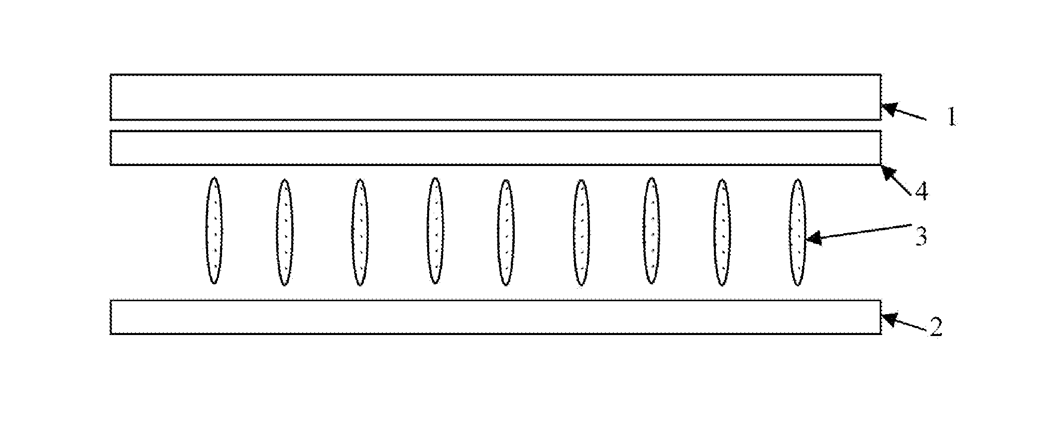
[0058]Referring to FIG. 6, a TN-type touch control liquid crystal display device according to the embodiment of the invention includes a color film substrate T11, a thin film transistor array substrate T13, and a liquid crystal layer T12 arranged between the color film substrate T11 and the thin film transistor array substrate T13.

[0059]Where the color film substrate T11 includes a glass substrate T111, a grid-shaped black matrix layer T1121, a touch control layer and a color film layer T114 in that order and further includes a planar layer T115 below the color film layer T114 and a common electrode T116 below the planar layer T115;

[0060]The thin film transistor array substrate T13 is composed of pixel electrodes, a thin film transistor array layer T131 and a glass substrate T132;

[0061]The touch control layer includes a first metal layer T1122, an insulation layer T1123 and a second metal layer T113;

[0062]Specifically, reference is made to FIG. 7(a) illustrating a structural top vie...

second embodiment

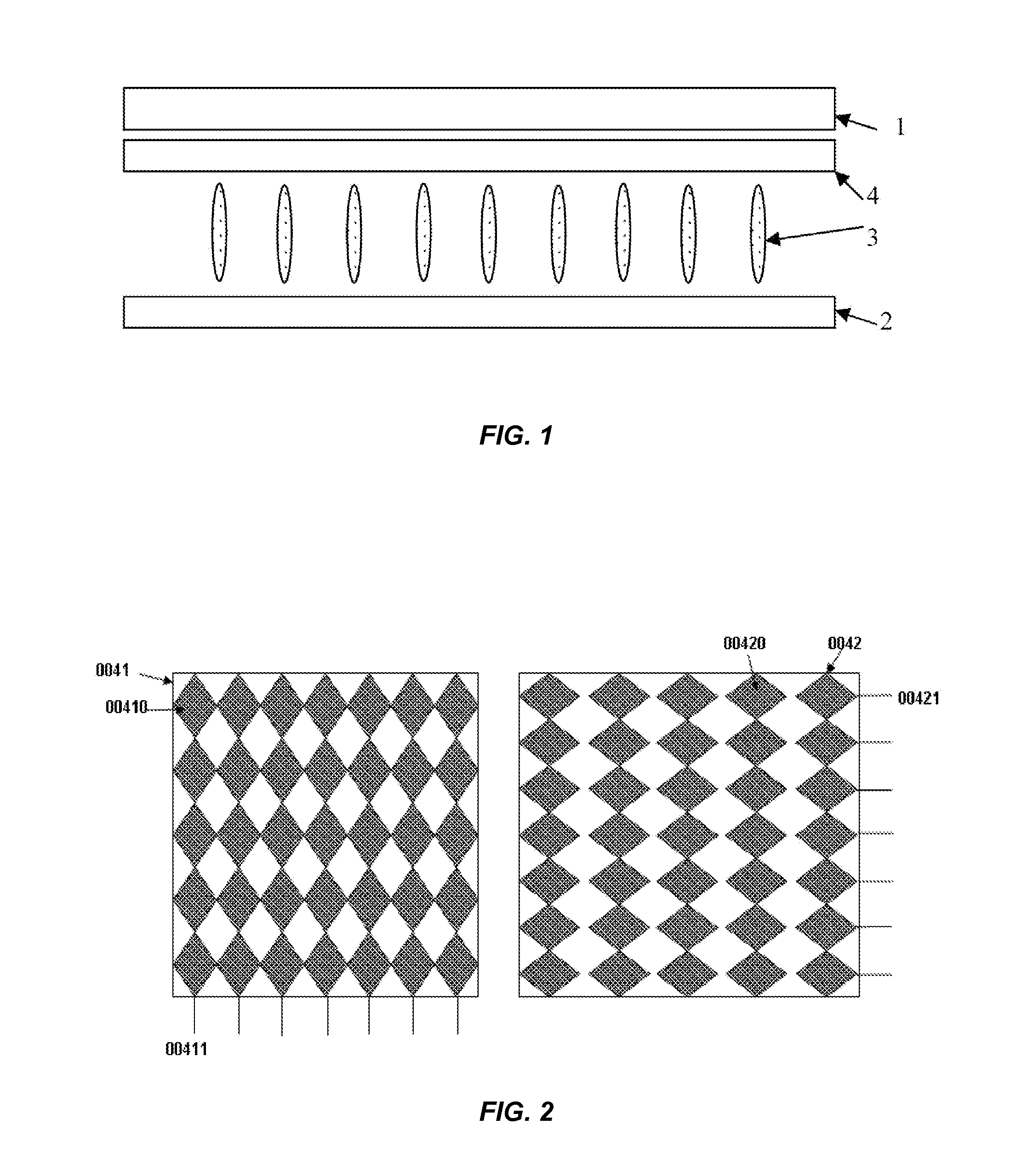
[0082]In the present second embodiment, unlike the structure of the touch control layer according to the foregoing first embodiment, specifically a first metal layer includes drive electrodes, sense electrodes and second metal connection lines; and a second metal layer includes first metal connection lines. This variant of the structure will neither influence an implementation of the technical solution of the invention nor influence the advantageous effects thereof. Specifically the structure thereof is as illustrated in FIG. 11(a) and FIG. 11(c);

[0083]FIG. 11(a) is a structural top view of the touch control layer according to the second embodiment, and as illustrated in FIG. 11(a), the touch control layer includes a plurality of drive electrodes 401 and sense electrodes 403 arranged in a rectangle, and the plurality of drive electrodes 401 are connected together through first metal connection lines 404 in the X direction to form a plurality of rows of drive electrodes, and the plur...

third embodiment

[0086]In the present third embodiment, a description will be given also taking a TN-type touch control liquid crystal display device as an example, where unlike the first embodiment and the second embodiment, the structure of the touch control layer in the third embodiment includes a first insulation layer, an insulation layer and a second metal layer; and the first metal layer includes drive electrodes and first metal connection lines, and the second metal includes sense electrodes and second metal connection lines. This variant of the structure will neither influence an implementation of the technical solution of the invention nor influence the advantageous effects thereof. Specifically the structure thereof is as illustrated in FIG. 12(a) and FIG. 12(c);

[0087]As illustrated in FIG. 12(a), the touch control layer includes a plurality of drive electrodes 501 and sense electrodes 503 arranged in a rectangle, and the plurality of drive electrodes 501 are connected together through fi...


PUM


Abstract

One inventive aspect is a touch control liquid crystal display device. The device includes a color film substrate, a thin film transistor array substrate, and a liquid crystal layer between the color film substrate and the thin film transistor array substrate. The color film substrate includes a grid-shaped black matrix layer, a touch control layer, and a color film layer. The touch control layer includes metal grid electrodes in a rectangle, where the metal grid electrodes include metal lines intersecting transversely and vertically. In addition, the metal grid electrodes include drive electrodes and sense electrodes. The drive electrodes are connected together through first metal connection lines in a first direction, and the sense electrodes are connected together through second metal connection lines in a second direction. In addition, the projection of the metal grid electrodes falls into the projection of the black matrix layer in the light transmission direction.

Description

CROSS-REFERENCES TO RELATED APPLICATIONS[0001]This application claims the benefit of priority to Chinese Patent Application No. 201210545803.6, filed with the Chinese Patent Office on Dec. 14, 2012, entitled “Touch Control Liquid Crystal Display Device”, the contents of which is incorporated herein by reference in its entirety.TECHNICAL FIELD[0002]The present invention relates to the field of touch display technologies and particularly to a touch control liquid crystal display device.BACKGROUND OF THE INVENTION[0003]A touch screen which is an input medium is the most simple, convenient and natural human-machine interaction means at present. Thus touch screens have been increasingly applied to various electronic products, e.g., a mobile phone, a notebook computer, an MP3 / MP4, etc.[0004]FIG. 1 is a touch control liquid crystal display device in the prior art, and as illustrated, the touch control liquid crystal display device includes a substrate 2, a color film substrate 1, and a liq...

Claims


Application Information

Patent Timeline
IPC IPC(8): G02F1/1333
CPCG02F1/13338G06F3/0412G06F3/044G02F1/133512G06F3/0443G06F3/0446
Inventor WANG, LIHUAMA, CONGHUAYAO, QIJUNMA, JUN
Owner SHANGHAI TIANMA MICRO ELECTRONICS CO LTD
Why Eureka
Try Eureka