Functional panel, device, and data processor

a technology of functional panels and data processors, applied in the field of functional panels, a device, or a data processor, to achieve the effect of high convenient or reliable, highly convenient or reliabl

Active Publication Date: 2016-04-14
SEMICON ENERGY LAB CO LTD
View PDF5 Cites 18 Cited by
  • Summary
  • Abstract
  • Description
  • Claims
  • Application Information

AI Technical Summary

Benefits of technology

[0008]An object of one embodiment of the present invention is to provide a novel functional panel that is highly convenient or reliable. Another object of one embodiment of the present invention is to provide a novel device that is highly convenient or reliable. Another object of one embodiment of the present invention is to provide a novel functional panel, a novel device, or a novel semiconductor device.

Problems solved by technology

For example, portable data processors are often used while being carried around by a user, and force might be accidentally applied, by dropping, to the data processors and display devices included in them.

Method used


Image

  • Functional panel, device, and data processor
  • Functional panel, device, and data processor
  • Functional panel, device, and data processor

Examples


embodiment 1

[0063]In this embodiment, the structure of a functional panel of one embodiment of the present invention will be described with reference to FIGS. 1A to 1D, FIGS. 2A and 2B, FIGS. 3A and 3B, and FIGS. 4A and 4B.

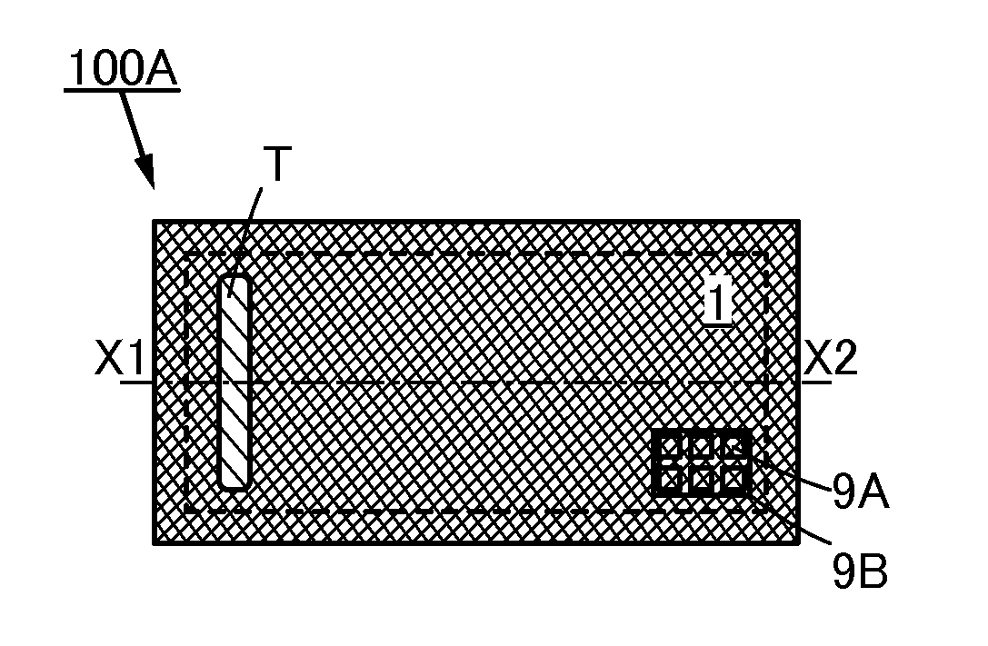
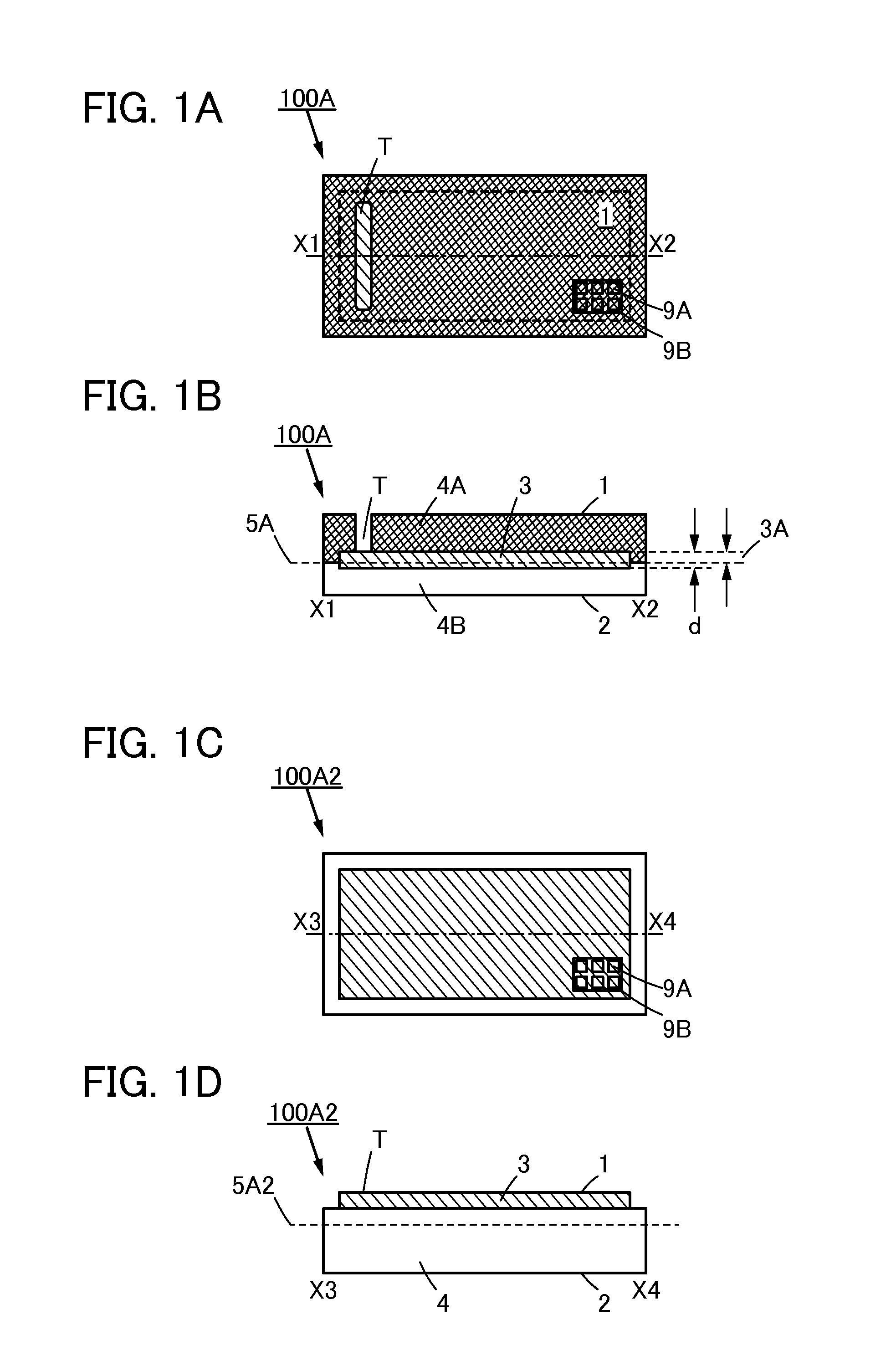
[0064]FIGS. 1A to 1D illustrate the structures of functional panels of embodiments of the present invention. FIG. 1A is a top view of a functional panel 100A of one embodiment of the present invention, and FIG. 1B is a cross-sectional view taken along the line X1-X2 in FIG. 1A.

[0065]FIG. 1C is a top view of a functional panel 100A2 of one embodiment of the present invention, and FIG. 1D is a cross-sectional view taken along the line X3-X4 in FIG. 1C.

[0066]The functional panel 100A described in this embodiment includes a first plane 1, a second plane 2 that is opposite the first plane 1, a neutral plane 5A in a region between the first plane 1 and the second plane 2, a functional layer 3 at least a portion 3A of which is in a region between the first plane 1 and the neutral pl...

embodiment 2

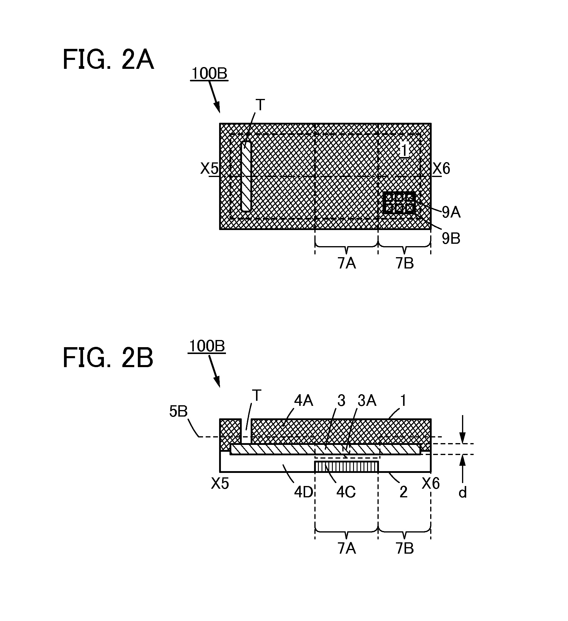
[0140]In this embodiment, the structure of a device of one embodiment of the present invention will be described with reference to FIGS. 5A to 5D, FIGS. 6A to 6D, FIGS. 7A to 7C, and FIGS. 8A to 8D.

[0141]FIGS. 5A to 5D illustrate the structure of a device of one embodiment of the present invention. FIG. 5A is a projection view illustrating a device 200A of one embodiment of the present invention which is bent, and FIG. 5B is a cross-sectional view taken along the line Y1-Y2 in FIG. 5A. FIG. 5C is a projection view illustrating the device 200A of one embodiment of the present invention which is unbent, and FIG. 5D is a cross-sectional view taken along the line Y3-Y4 in FIG. 5C.

[0142]FIGS. 6A to 6D illustrate a hinge portion that can be used in the device of one embodiment of the present invention. FIG. 6A is a side view illustrating the structure of a hinge portion 213 in a bent state, and FIG. 6B is a side view illustrating the structure of the hinge portion 213 in an unbent state.

[...

embodiment 3

[0174]In this embodiment, a method of manufacturing a stack that can be used in the manufacture of the functional panel of one embodiment of the present invention will be described with reference to FIGS. 9A-1 and 9A-2, FIGS. 9B-1 and 9B-2, FIG. 9C, FIGS. 9D-1 and 9D-2, and FIGS. 9E-1 and 9E-2.

[0175]FIGS. 9A-1 to 9E-2 are schematic views illustrating a process of manufacturing the stack. Cross-sectional views illustrating structures of a processed member and the stack are shown on the left side of FIGS. 9A-1 to 9E-2, and top views corresponding to the cross-sectional views except FIG. 9C are shown on the right side.

[0176]A method of manufacturing a stack 81 from a processed member 80 will be described with reference to FIGS. 9A-1 to 9E-2.

[0177]The processed member 80 includes a first substrate F1, a first separation layer F2 on the first substrate F1, a first layer F3 to be separated whose one surface is in contact with the first separation layer F2, a bonding layer 30 whose one sur...


PUM


Abstract

A novel functional panel, a novel device, or a novel data processor is provided. A structure in which a first plane, a second plane that is opposite the first plane, and a neutral plane between the first plane and the second plane are provided and a portion of a functional layer having a thickness greater than or equal to half of the thickness of the functional layer is in a region between the first plane and the neutral plane was conceived.

Description

BACKGROUND OF THE INVENTION[0001]1. Field of the Invention[0002]One embodiment of the present invention relates to a functional panel, a device, or a data processor.[0003]Note that one embodiment of the present invention is not limited to the above technical field. The technical field of one embodiment of the invention disclosed in this specification and the like relates to an object, a method, or a manufacturing method. In addition, one embodiment of the present invention relates to a process, a machine, manufacture, or a composition of matter. Specifically, examples of the technical field of one embodiment of the present invention disclosed in this specification include a semiconductor device, a display device, a light-emitting device, a power storage device, a memory device, a method for driving any of them, and a method for manufacturing any of them.[0004]2. Description of the Related Art[0005]The social infrastructures relating to means for transmitting information have advance...

Claims


Application Information

Patent Timeline
Patent Type & Authority Applications(United States)
IPC IPC(8): G06F3/041G06F1/16
CPCG06F3/0412G06F2203/04102G06F1/16G06F1/1616G06F1/163G06F1/1681G06F2203/04103G06F1/1626G06F1/1641G06F1/1652G06F3/0446G06F2203/04112Y02P70/50
Inventor JINBO, YASUHIROENDO, AKIO
Owner SEMICON ENERGY LAB CO LTD
Why Eureka
Try Eureka