Touch panel
a technology of touch panel and touch panel, applied in the field of touch panel, can solve the problems of not being able to achieve higher translucency and not being easily formed to be thin, and achieve the effect of effective arrangemen
- Summary
- Abstract
- Description
- Claims
- Application Information
AI Technical Summary
Benefits of technology
Problems solved by technology
Method used
Image
Examples
first embodiment
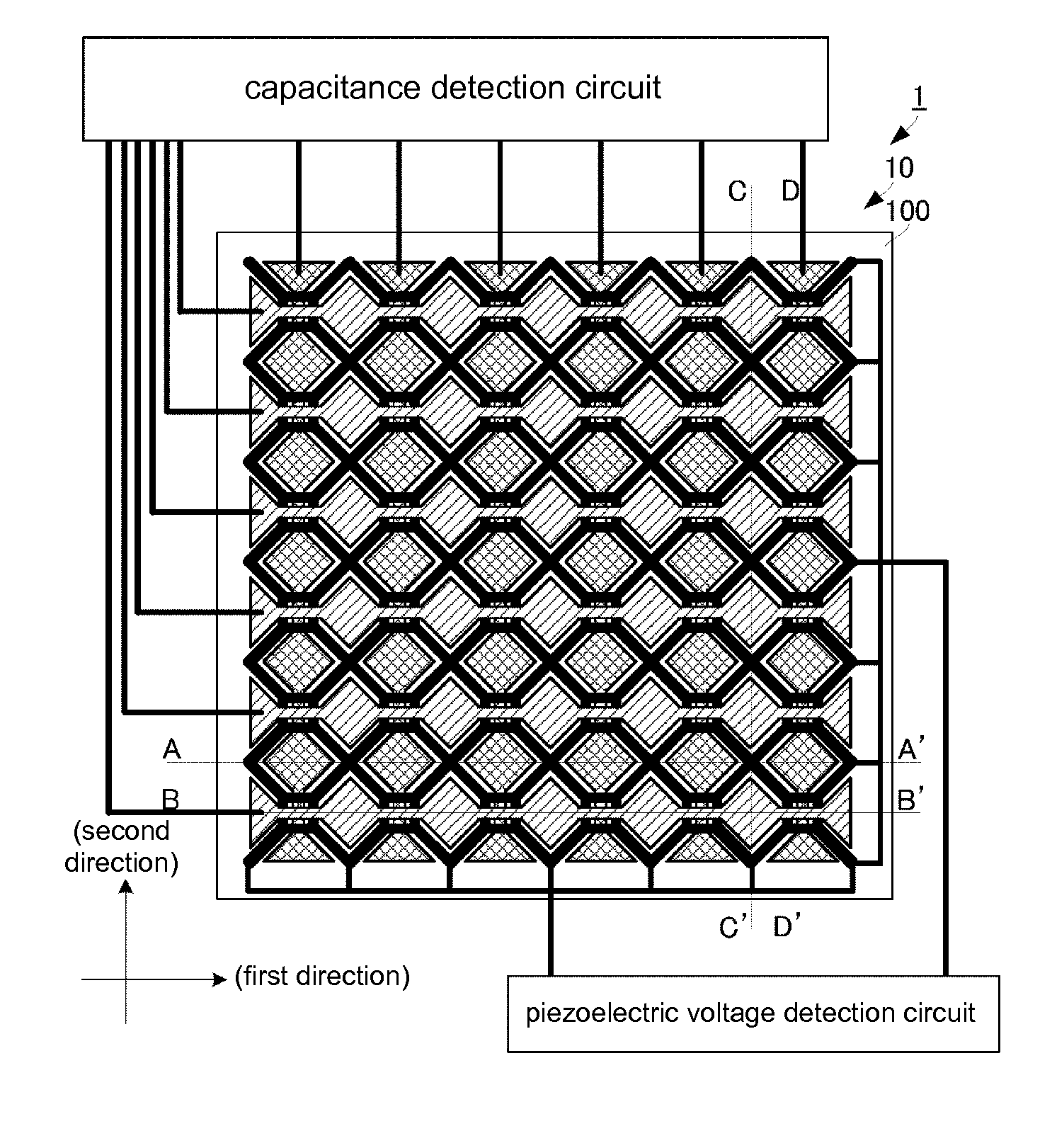
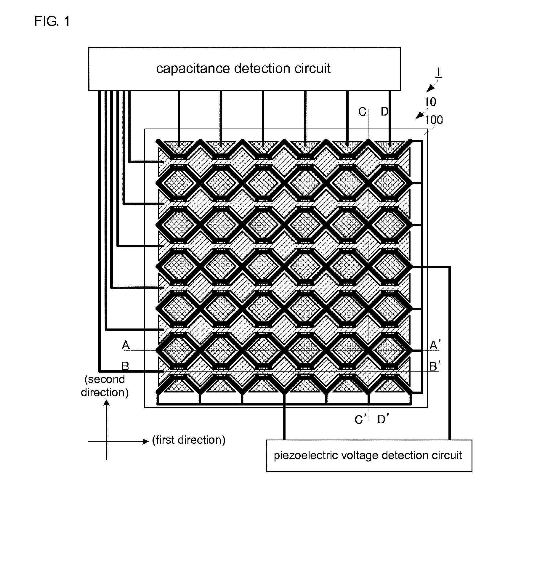
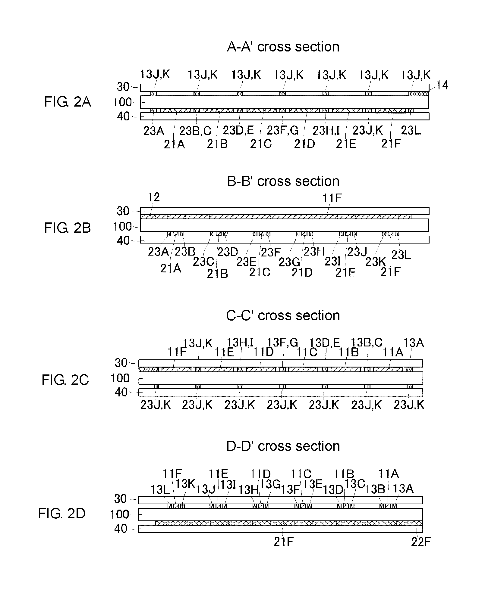
[0127]On the first principal surface 100ST of the piezoelectric film 100, the first capacitance detection sub-electrodes 11A to 11F are formed as shown in FIG. 9. Although the first capacitance detection sub-electrodes 11A to 11F have the same structure as in the first embodiment, those are formed such that the extending direction of the first capacitance detection sub-electrodes 11A to 11F is in parallel with the uniaxially stretched direction 900 (first direction).
[0128]First piezoelectric voltage detection sub-electrodes 131A, 132A are formed along the outer diameter shape of the first capacitance detection sub-electrode 11A on the opposite side to the first capacitance detection sub-electrode 11B, as spaced from the first capacitance detection sub-electrode 11A. The first piezoelectric voltage detection sub-electrodes 131A, 132A are separated at the midpoint along the first direction, and one end side from the separation point 150 along the first direction becomes the first piez...
fifth embodiment
[0200]On the first principal surface 100ST of the piezoelectric film 100, the first piezoelectric voltage detection sub-electrodes 13A′ to 13H′ and the first piezoelectric voltage detection sub-electrodes 13A′ to 13H′ are arrayed and formed as in the principal function section 10D of the touch panel of the
[0201]A protective layer 30″ is formed substantially all over the surface of the first principal surface 100ST of the piezoelectric film 100 formed with the first capacitance detection sub-electrodes 11A′ to 11I′ and the surface of the first piezoelectric voltage detection sub-electrodes 13A′ to 13H′.
[0202]On the surface (surface on the opposite side to the piezoelectric film 100) of the protective layer 30″, the second capacitance detection sub-electrodes 21A′ to 21K′ are formed.
[0203]Even with such a structure formed, the touched position and the pressed amount (pressed force) can be detected simultaneously as in each of the foregoing embodiments. A thin touch panel with high tra...
PUM
 Abstract
Description
Claims
Application Information


