Method for transferring device

a technology of transferring device and transferring device, which is applied in the direction of layered product treatment, chemistry apparatus and processes, layered products, etc., can solve problems such as integration and packaging, and achieve the effect of reducing adhesion for

Inactive Publication Date: 2016-05-26
MIKRO MESA TECH
View PDF6 Cites 38 Cited by
  • Summary
  • Abstract
  • Description
  • Claims
  • Application Information

AI Technical Summary

Benefits of technology

[0006]In one embodiment, a method for transferring at least one device is provided. The method includes: coating a first adhesive layer onto a first carrier substrate; putting the device onto the first adhesive layer, such that the first adhesive layer temporarily adheres the device thereto; reducing adhesion force of the first adhesive layer to the device while remaining the device within a controllable region on the first adhesive layer, in which the first adhesive layer has a Young's modulus less than or equal to 30 GPa; and transferring the device from the first adhesive layer to a receiving substrate after the adhesion force of the first adhesive layer is reduced.

Problems solved by technology

Integration and packaging issues are one of the main obstacles for the commercialization of micro devices such as radio frequency (RF) microelectromechanical systems (MEMS) microswitches, light-emitting diode (LED) display systems, and MEMS or quartz-based oscillators.

Method used


Image

  • Method for transferring device
  • Method for transferring device
  • Method for transferring device

Examples


Embodiment Construction

[0015]In the following detailed description, for purposes of explanation, numerous specific details are set forth in order to provide a thorough understanding of the disclosed embodiments. It will be apparent, however, that one or more embodiments may be practiced without these specific details. In other instances, well-known structures and devices are schematically depicted in order to simplify the drawings.

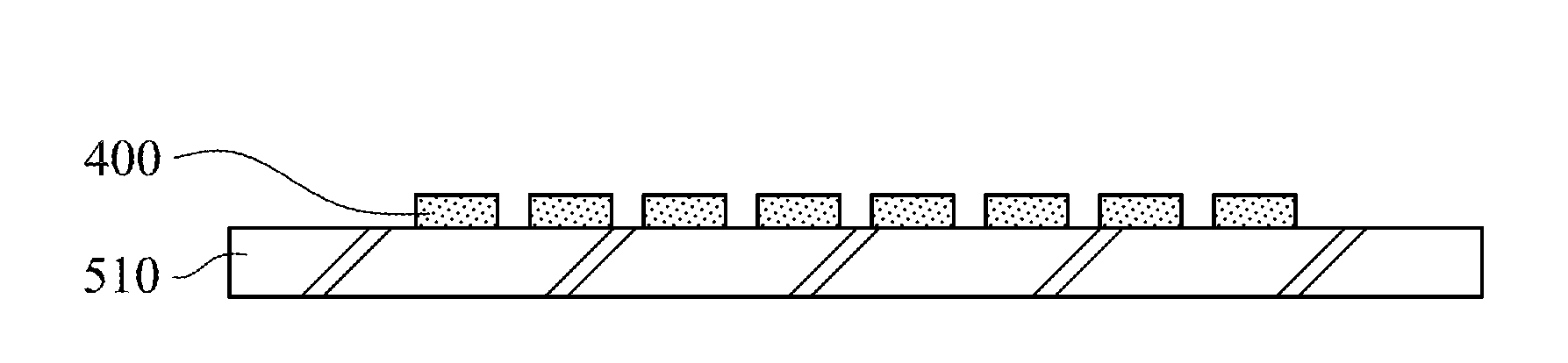
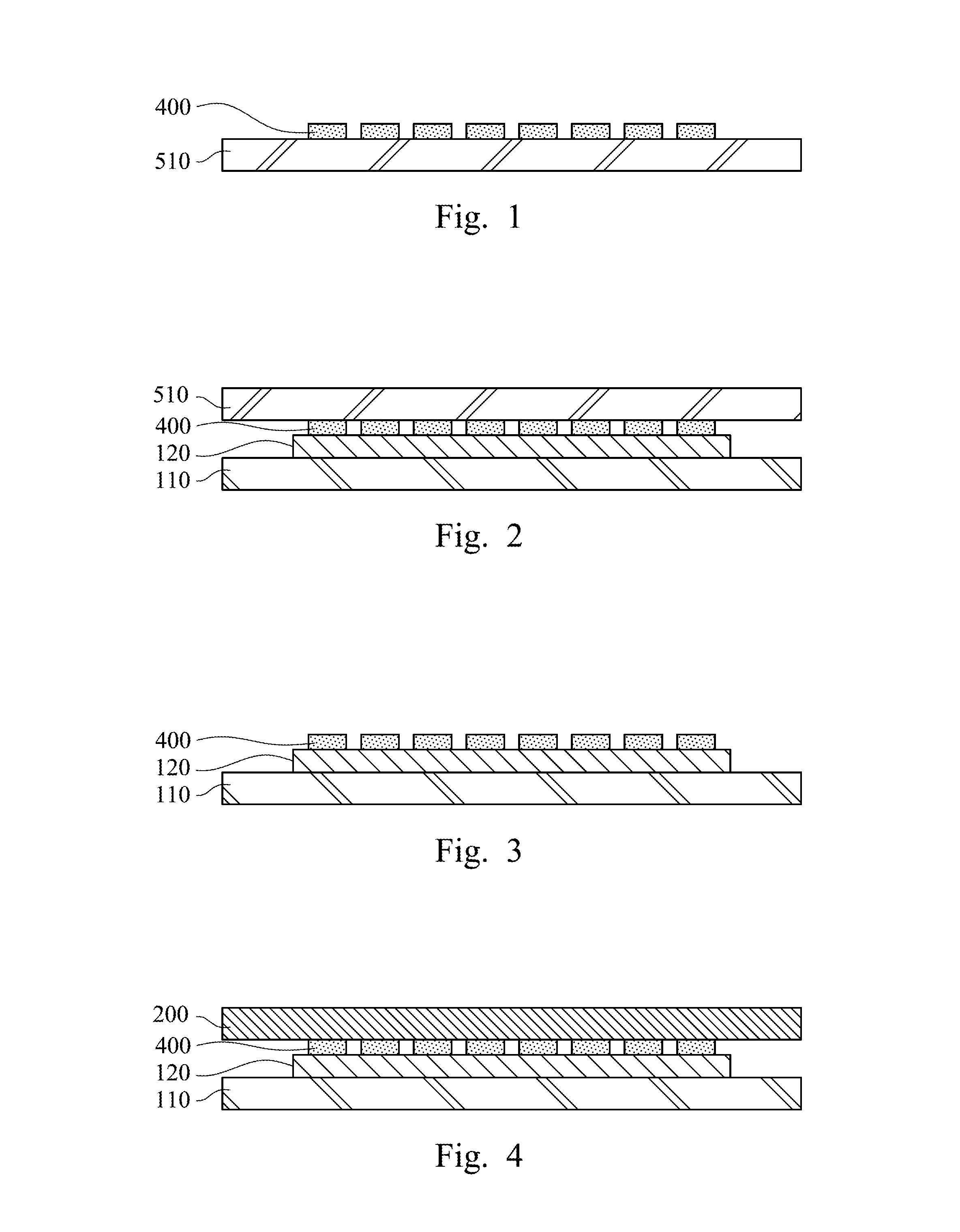
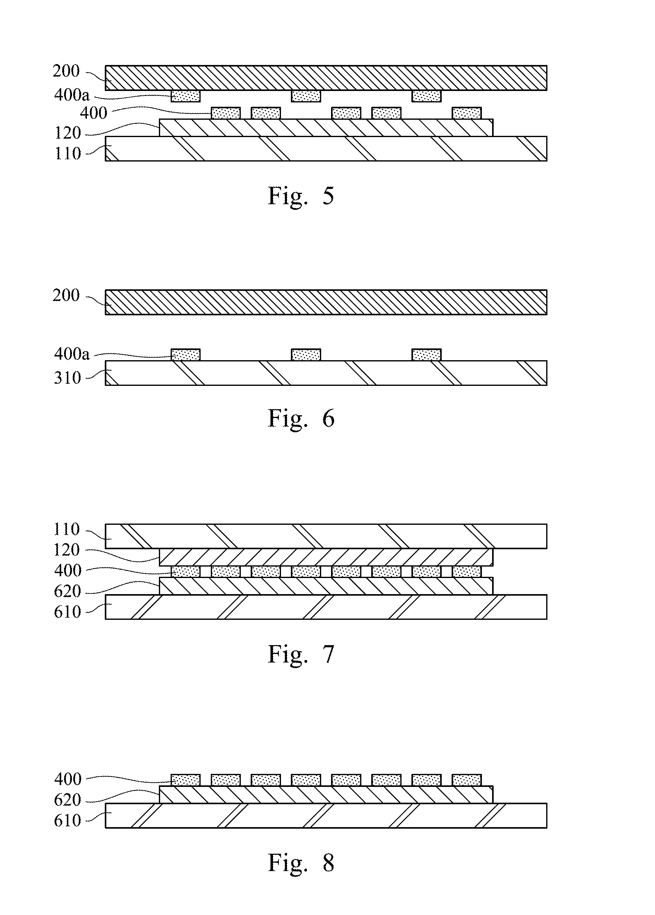
[0016]FIGS. 1 to 6 are cross-sectional views of intermediate steps in a method for transferring at least one device 400 according to one embodiment of this disclosure. A method for transferring at least one device 400 is provided. Specifically, the device 400 is a light emitting diode (LED). More specifically, the device 400 is a thin LED. The thickness of the device 400 may be in a range from about 0.5 μm to about 100 μm. The device 400 may be a cylindrical column, and the radius of the device 400 may be in a range from about 0.5 μm to about 500 μm. Embodiments of this disclosu...


PUM

PropertyMeasurementUnit
Young's modulusaaaaaaaaaa
thicknessaaaaaaaaaa
thicknessaaaaaaaaaa

Abstract

A method for transferring at least one device is provided. The method includes: coating a first adhesive layer onto a first carrier substrate; putting the device onto the first adhesive layer, such that the first adhesive layer temporarily adheres the device thereto; reducing adhesion force of the first adhesive layer to the device while remaining a location of the device in a controllable region on the first adhesive layer, wherein the first adhesive layer has a Young's modulus less than or equal to 30 GPa before and after the adhesion force of the first adhesive layer is reduced; and transferring the device from the first adhesive layer to a receiving substrate after the adhesion force of the first adhesive layer is reduced.

Description

BACKGROUND[0001]1. Technical Field[0002]The present disclosure relates to a method for transferring at least one device.[0003]2. Description of Related Art[0004]Integration and packaging issues are one of the main obstacles for the commercialization of micro devices such as radio frequency (RF) microelectromechanical systems (MEMS) microswitches, light-emitting diode (LED) display systems, and MEMS or quartz-based oscillators.[0005]Traditional technologies for transferring of devices include transfer by wafer bonding from a transfer wafer to a receiving wafer. One such implementation is “direct printing” involving one bonding step of an array of devices from a transfer wafer to a receiving wafer, followed by removal of the transfer wafer. Another such implementation is “transfer printing” involving two bonding / de-bonding steps. In transfer printing, a transfer wafer may pick up an array of devices from a donor wafer, and then bond the array of devices to a receiving wafer, followed ...

Claims


Application Information

Patent Timeline
Patent Type & Authority Applications(United States)
IPC IPC(8): B32B38/10B32B37/12
CPCB32B38/10B32B2309/105B32B37/12H01L21/67703H01L21/6836H01L2221/68313H01L2221/68363H01L21/6835H01L24/75H01L2224/7565H01L2224/7598H01L2221/68354H01L2221/68368H01L2221/68381H01L33/0093
Inventor CHANG, PEI-YU
Owner MIKRO MESA TECH
Why Eureka
Try Eureka