Electronic system modules and method of fabrication

a technology of electronic system module and fabrication method, which is applied in the direction of resist details, sustainable manufacturing/processing, and final product manufacturing, etc., can solve the problems of not being able to support direct mounting of bumped devices at a pitch of 100 microns, and not being able to meet the requirements of conventional testing methods, etc., to achieve excellent dimensional stability, the effect of avoiding the use of epoxy under layers and reducing

Inactive Publication Date: 2005-08-09
SK HYNIX INC
View PDF16 Cites 83 Cited by
  • Summary
  • Abstract
  • Description
  • Claims
  • Application Information

AI Technical Summary

Benefits of technology

[0019]A glass substrate for 5th generation fabrication of LCD circuits is typically 1100 by 1250 mm in area, and 1.1 mm thick, which can be used in carrying out the present invention. However, the glass carrier of the current invention can be of any size. The unit manufacturing costs of interconnection circuits and related circuit assemblies of the current invention are lower if larger glass panels are used. The glass or other rigid carrier provides mechanical support for all of the fabrication, component assembly, test, and rework process steps, and also has excellent dimensional stability. This dimensional stability transfers to the multi-layer circuits that are built up as a series of films on top of the glass. This transferred dimensional stability is a primary reason that fine line features such as trace widths less than 5 microns are possible with the current invention. It is also important however, that the final version of the interconnection circuit be flexible, because the flexibility allows the use of epoxy under layers to be avoided, leading to more robust rework processes for removing and replacing defective chips. The flexibility also allows system boards to be folded in compact devices such as cellular phones.
[0020]A release agent is applied to a glass panel substrate, except for a clear region near the edges. The clear region is characterized by high adhesion between the glass and the polymer base layer to be subsequently formed on the glass. The high adhesion region provides an anchor that firmly attaches the polymer to the glass around the perimeter of the panel. The release layer creates low adhesion between glass and polymer, so that after a circuit assembly has been built on top, it can be readily peeled off.
[0023]The glass carrier is diced with a diamond saw to separate individual circuit assemblies from one another, and provide a more convenient form for component assembly, test, and rework. The interconnection circuit itself must be tested, before any assembly is done. This test is performed using a test fixture that connects through a module access port to an external tester. The module access port may include I / O pads (module access pads) for every node of the multilayer interconnection circuit. The assembly and rework steps require that IC chips and other surface mounted components are precisely located in order that the bonding tool can accurately align bonding sites on the components with corresponding bonding sites on the interconnection circuit. Accordingly, the circuit assembly remains attached to the glass carrier, and its dimensional accuracy is maintained until these steps are completed.
[0024]A module cable with high-density interconnections is attached to each circuit assembly. The circuit assemblies are then separated from their individual glass carriers by peeling the base substrate away from the carrier. Since the adhesion force is low in these regions, they can be separated without damage.
[0025]Additional metal coatings are applied to create a circuit module that is hermetically sealed and electro-magnetically shielded. To effectively cool the dense circuit module, it may be bonded to a heat sink, and the heat sink may be cooled with a circulating fluid.

Problems solved by technology

None of the available printed circuit board technologies can support direct mounting of bumped devices at a pitch of 100 microns or less.
However, the application of IC chip manufacturing facilities to this problem is more than what is required.
This flexibility, wherein the assembly process is tailored to yield issues in real time, is not available with conventional testing methods.
This contrasts with conventional methods requiring component test, sub-assembly test, and system test, with numerous iterations if problems develop.
This makes it more difficult to test remotely through a cable, and still achieve the necessary noise margins.
Such a unified process has only recently become feasible.
The process of cleaning off the residue has typically resulted in damage to the fine pitch bonding sites, to the point where they cannot be reliably re-bonded.
A related issue is the recent requirement for low stress in IC chips that use ultra-low-k dielectric materials.

Method used


Image

  • Electronic system modules and method of fabrication
  • Electronic system modules and method of fabrication
  • Electronic system modules and method of fabrication

Examples


Embodiment Construction

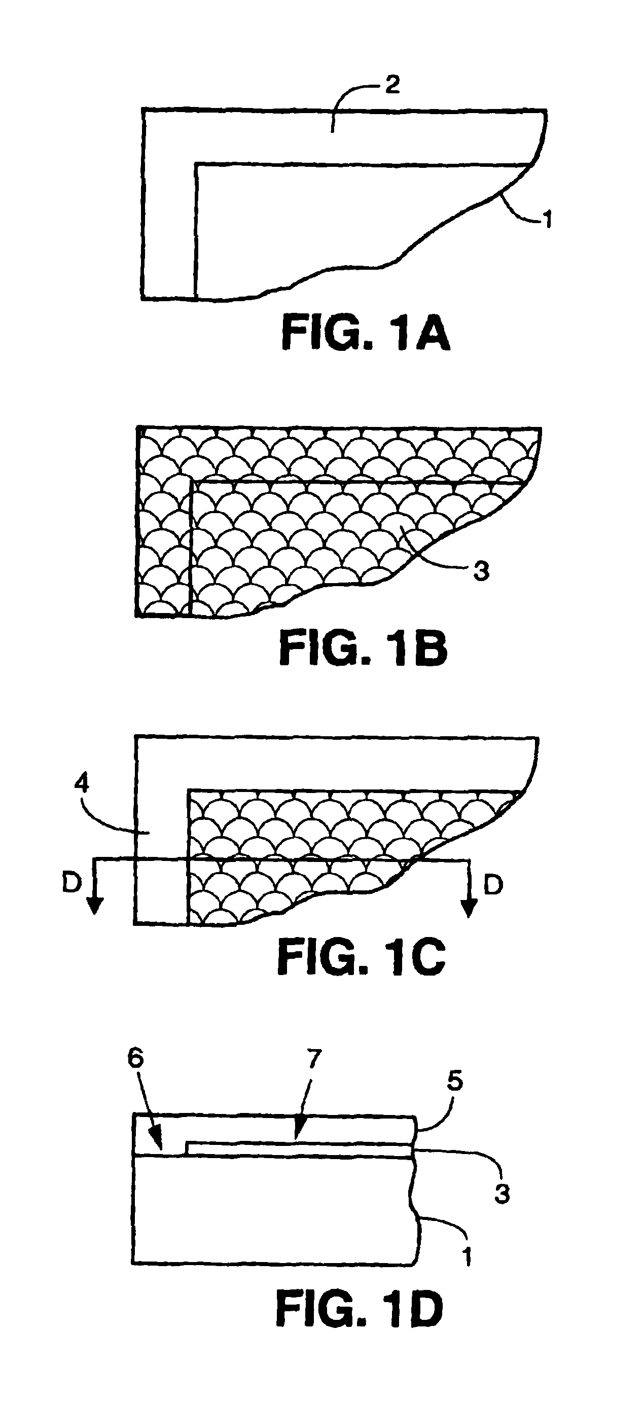
[0054]FIG. 1A shows a corner fragment of a glass carrier 1. Photo resist has been patterned on the carrier, so that a border of resist, 2, having a width of approximately 20 mm, surrounds the perimeter. FIG. 1B shows that a film of release layer, 3, has been applied over the entire surface of the glass carrier. A suitable material for the release layer is a fluorinated silicone such as F065 manufactured by Gelest, Inc., in Morrisville Pa., USA. This material is a single part gel. It can be applied as a fog or fine spray, or using the spin-on method. A suitable thickness is 2-5 microns after curing, with 2 microns preferred. A typical curing cycle is 125° C. for 25 minutes. This release material has a silane component that bonds well to glass surfaces, yet presents a fluid-like interface to polymeric materials like the base layer to be subsequently applied. FIG. 1C shows the result of lifting the resist to pattern the release layer, using a developer or resist stripper to swell the r...


PUM


Abstract

This specification describes techniques for manufacturing an electronic system module. The module includes flexible multi-layer interconnection circuits with trace widths of 5 microns or less. A glass panel manufacturing facility, similar to those employed for making liquid crystal display, LCD, panels is used to fabricate the interconnection circuits. A polymer base layer is formed on a glass carrier with an intermediate release layer. Alternate layers of metal and dielectric are formed on the base layer, and patterned to create an array of multi-layer interconnection circuits on the glass panel. A thick layer of polymer is deposited on the interconnection circuit, and openings formed at input / output (I / O) pad locations. Solder paste is deposited in the openings to form wells filled with solder. After dicing the glass carrier to form separated interconnection circuits, IC chips are stud bumped and assembled using flip chip bonding, wherein the stud bumps on the components are inserted into corresponding wells on the interconnection circuits. The IC chips are tested and reworked to form tested circuit assemblies. Methods for connecting to testers and to other modules and electronic systems are described. Module packaging layers are provided for hermetic sealing and for electromagnetic shielding. A blade server embodiment is also described.

Description

RELATED APPLICATIONS[0001]This application claims priority to Provisional Application Ser. No. 60 / 318,271 filed Sep. 7, 2001.BACKGROUND OF THE INVENTION[0002]1. Field of the Invention[0003]This invention relates generally to an electronic system module and method of fabrication, and more particularly to an electronic system module fabricated on a carrier from which it can be released.[0004]2. Description of the Related Art[0005]The number of input / output (I / O) connections required by integrated circuit (IC) chips is increasing, to several hundred for recent microprocessor chips. As verification of complex designs becomes an increasing portion of the total design activity, it is desirable to increase the I / O count further, to provide access to more internal nodes for testing. Flip chip assembly methods have helped to provide more I / O connections because they provide an area array of connections across the entire face of an IC chip, rather than just at the perimeter as with wire bondi...

Claims


Application Information

Patent Timeline
Patent Type & Authority Patents(United States)
IPC IPC(8): H01L23/538H01L23/52H01L23/498H01L23/48H05K3/46H05K1/00H05K1/11H05K3/34H05K3/00
CPCH01L23/49811H01L23/5387H01L24/16H05K1/0289H05K1/115H05K3/3436H05K3/4682H01L23/5386H01L2224/73204H01L2224/1134H01L2224/13144H01L2924/01013H01L2924/01015H01L2924/01018H01L2924/01027H01L2924/01029H01L2924/01039H01L2924/01051H01L2924/01074H01L2924/01075H01L2924/01078H01L2924/01079H01L2924/01082H01L2924/01327H01L2924/14H01L2924/3011H01L2924/3025H05K3/007H05K3/3484H05K2201/0379H05K2201/09472H05K2201/09509H05K2201/10674H05K2203/016H05K2203/0568H01L2224/45144H01L2224/45015H01L24/25H01L2924/014H01L2924/01033H01L2924/01019H01L2924/01006H01L2924/01005H01L2924/00013H01L2224/16237H01L2924/00014H01L2224/13099H01L2224/29099H01L2924/20751H01L2924/00H01L2924/351H01L2924/15788H01L2224/05573H01L2224/05567H05K3/3485Y02P70/50
Inventor SALMON, PETER C.
Owner SK HYNIX INC
Why Eureka
Try Eureka