Display panel and display module

Inactive Publication Date: 2016-06-02
SEMICON ENERGY LAB CO LTD
View PDF4 Cites 24 Cited by
  • Summary
  • Abstract
  • Description
  • Claims
  • Application Information

AI Technical Summary

Benefits of technology

[0009]An object of one embodiment of the present invention is to provide a novel display panel with improved convenience or reliability, a novel display panel

Problems solved by technology

Functions of some functional elements ar

Method used


Image

  • Display panel and display module
  • Display panel and display module
  • Display panel and display module

Examples


embodiment 1

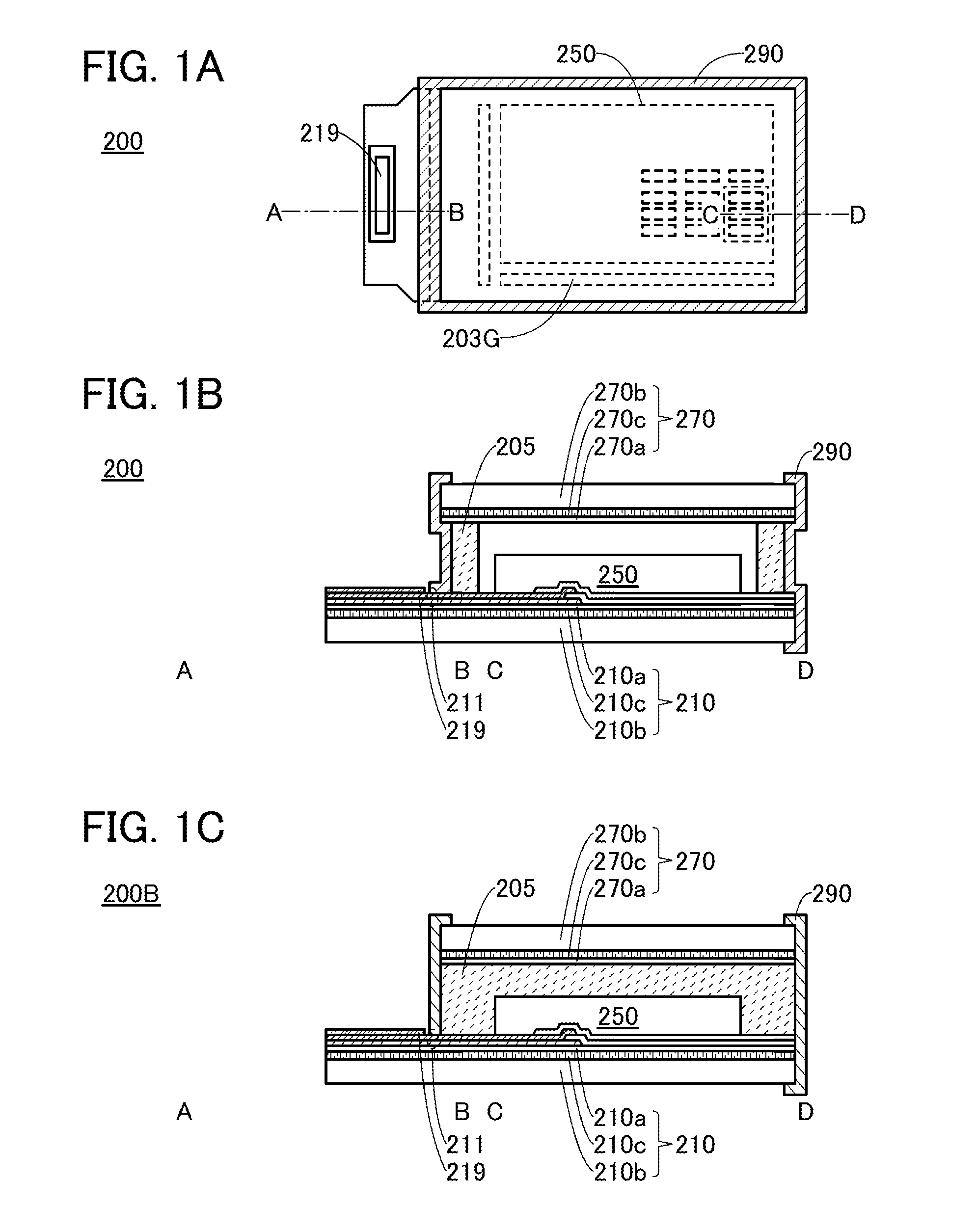
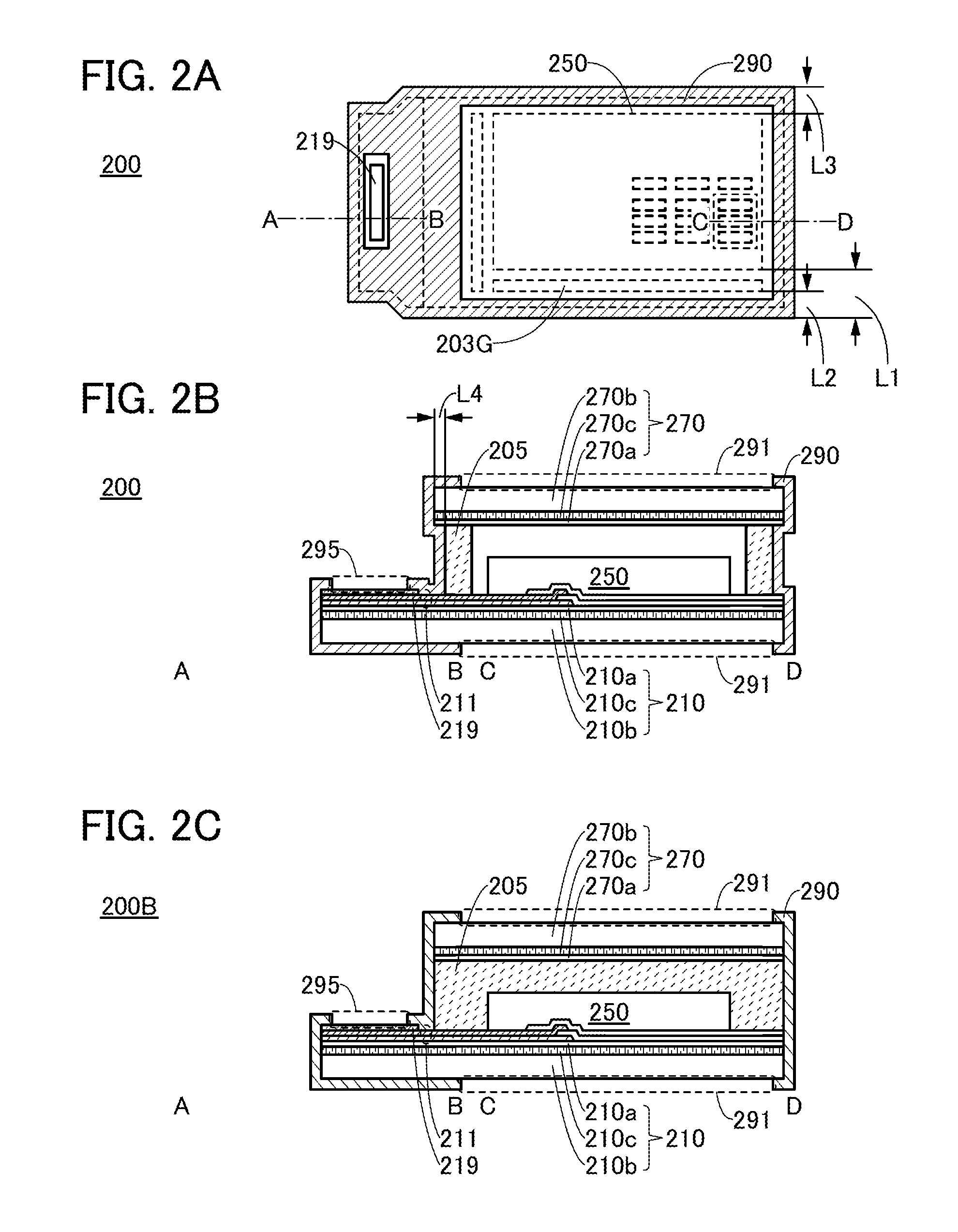
[0055]In this embodiment, the structure of a display panel of one embodiment of the present invention will be described with reference to the drawings.

[0056]FIGS. 2A to 2C illustrate the structures of a display panel of one embodiment of the present invention. FIG. 2A is a top view of a display panel 200 which is one embodiment of the present invention. FIG. 2B is a cross-sectional view taken along the line A-B and the line C-D in FIG. 2A.

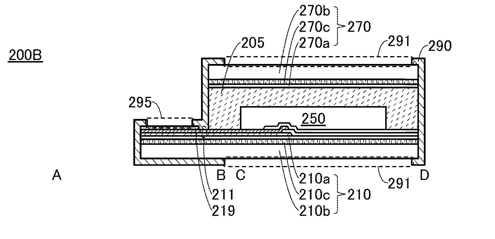
[0057]FIG. 2C is a cross-sectional view illustrating the structure of a display panel 200B which is different in structure from the display panel 200 shown in FIG. 2B.

[0058]The display panel 200 described in this embodiment includes a terminal 219, a first base 210 that supports the terminal 219, a second base 270 that has a region overlapping with the first base 210, a bonding layer 205 that bonds the first base 210 to the second base 270, a display element 250 that is between the first base 210 and the second base 270 and is electrically connecte...

embodiment 2

[0150]In this embodiment, the structures of a display module of one embodiment of the present invention will be described with reference to FIGS. 6A to 6C and FIGS. 7A to 7C.

[0151]FIGS. 6A to 6C illustrate the structures of a display module of one embodiment of the present invention. FIG. 6A is a top view of a display module 200M of one embodiment of the present invention. FIG. 6B is a cross-sectional view taken along the line A-B and the line C-D in FIG. 6A.

[0152]FIG. 6C is a cross-sectional view illustrating the structure of a display module 200 MB which is different in structure from the display module 200M shown in FIG. 6B.

[0153]The display module 200M described in this embodiment includes a terminal 219, a first base 210 that supports the terminal 219, a second base 270 that has a region overlapping with the first base 210, a bonding layer 205 that bonds the first base 210 to the second base 270, a display element 250 that is between the first base 210 and the second base 270 a...

embodiment 3

[0176]In this embodiment, methods for manufacturing a display panel of one embodiment of the present invention will be described with reference to FIG. 8, FIGS. 9A to 9C, FIGS. 10A and 10B, and FIGS. 11A and 11B.

[0177]FIG. 8 is a flow chart illustrating a method for manufacturing a display panel of one embodiment of the present invention.

[0178]FIGS. 9A to 9C illustrate a method for manufacturing a display panel of one embodiment of the present invention. Specifically, FIGS. 9A to 9C are cross-sectional views of the display panels during the manufacturing process.

>

[0179]A method for manufacturing a display panel described in this embodiment includes the following three steps (see FIG. 8).

>

[0180]In a first step, a processed member that includes the following components is prepared: the terminal 219, the first base 210 that supports the terminal 219, the second base 270 that has a region overlapping with the first base 210, the bonding layer 205 that bonds the first base 210 to the sec...


PUM


Abstract

A novel display panel excellent in convenience or reliability, or a novel display panel with excellent mountability on a housing is provided. The display panel includes a terminal, a first base that supports the terminal, the second base that has a region overlapping with the first base, a bonding layer that bonds the first base to the second base, a display element that is between the first base and the second base and is electrically connected to the terminal, and an insulating layer that is in contact with the first base, the second base, and the bonding layer. The insulating layer includes an opening in a region overlapping with the display element.

Description

BACKGROUND OF THE INVENTION[0001]1. Field of the Invention[0002]One embodiment of the present invention relates to a display panel. Another embodiment of the present invention relates to a display module.[0003]Note that one embodiment of the present invention is not limited to the above technical field. The technical field of one embodiment of the invention disclosed in this specification and the like relates to an object, a method, or a manufacturing method. In addition, one embodiment of the present invention relates to a process, a machine, manufacture, or a composition of matter. Specifically, examples of the technical field of one embodiment of the present invention disclosed in this specification include a semiconductor device, a display device, a light-emitting device, a power storage device, a memory device, a method for driving any of them, and a method for manufacturing any of them.[0004]2. Description of the Related Art[0005]Functions of some functional elements are impai...

Claims


Application Information

Patent Timeline
IPC IPC(8): G02F1/1345H01L27/32H01L51/56G02F1/1333H01L51/52
CPCG02F1/13452G02F1/133345H01L51/5246H01L2227/323H01L27/3276H01L2251/5338H01L51/56G02F1/13458G02F2201/501G02F1/13456H10K59/1213H10K59/131H10K77/111H10K50/841H10K50/8426H10K50/844H10K59/1201H10K2102/311H10K71/00
Inventor YAMAZAKI, SHUNPEIJINBO, YASUHIROOKAZAKI, KENICHI
Owner SEMICON ENERGY LAB CO LTD
Why Eureka
Try Eureka