Semiconductor light-emitting device

Active Publication Date: 2016-06-23
PLAYNITRIDE
View PDF28 Cites 1 Cited by
  • Summary
  • Abstract
  • Description
  • Claims
  • Application Information

AI Technical Summary

Benefits of technology

[0007]The invention provides a semiconductor light-

Problems solved by technology

However, in a conventional gallium nitride (GaN) LED, a band gap between a P-type GaN semiconductor layer and an N-type GaN semiconductor layer is approximate to a band gap of the l

Method used


Image

  • Semiconductor light-emitting device
  • Semiconductor light-emitting device
  • Semiconductor light-emitting device

Examples


Example

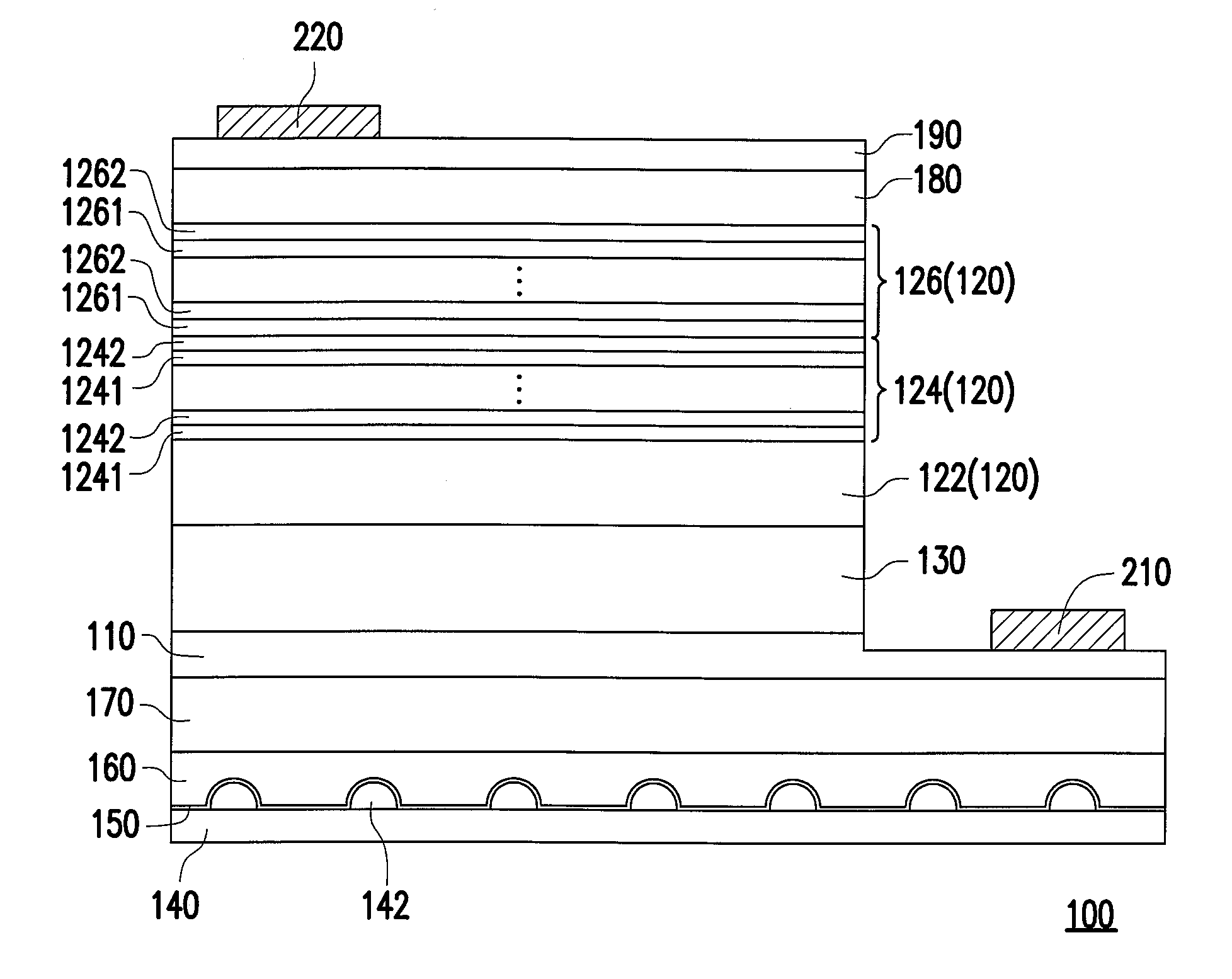
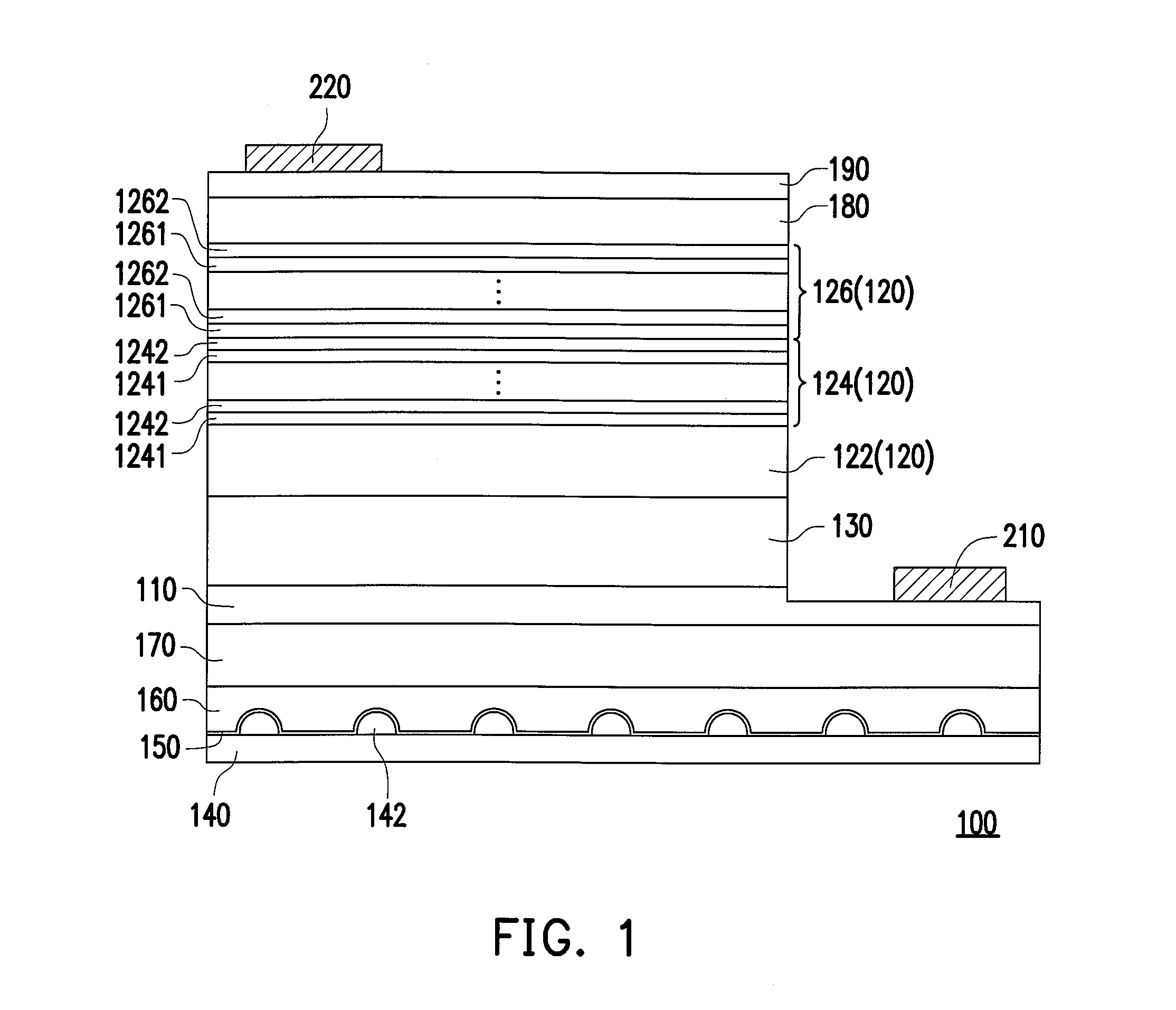
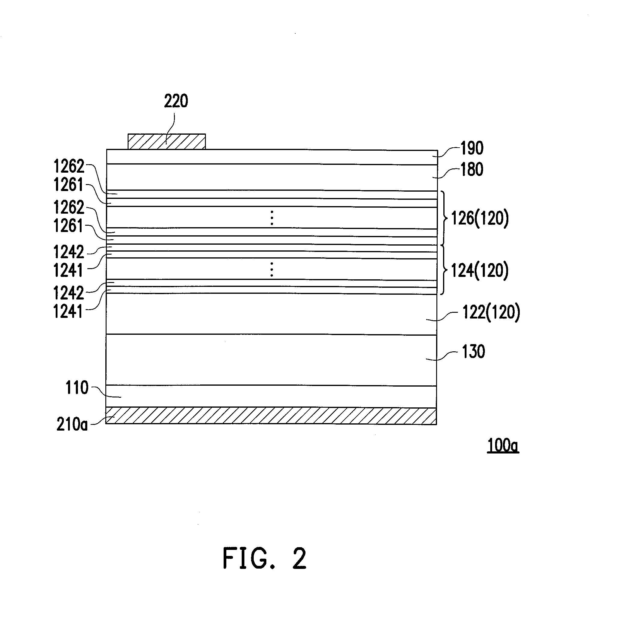
[0023]FIG. 1 is a cross-sectional diagram illustrating a semiconductor light-emitting device according to an embodiment of the invention. With reference to FIG. 1, a semiconductor light-emitting device 100 of the present embodiment includes an N-type semiconductor layer 110, a plurality of P-type semiconductor layers 120, a light-emitting layer 130 and a contact layer 180. The light-emitting layer 130 is disposed between the N-type semiconductor layer 110 and the whole of the P-type semiconductor layers 120. The P-type semiconductor layers 120 are disposed between the contact layer 180 and the light-emitting layer 130. Light emitted from the light-emitting layer 130 may include blue light, ultraviolet (UV) light or a combination thereof. In the present embodiment, the light-emitting layer 130 may be, for example, a multiple quantum well (MQW) layer formed by alternately stacking a plurality of N-type indium gallium nitride (InGaN) layers and a plurality of N-type gallium nitride (Ga...


PUM


Abstract

A semiconductor light-emitting device including an N-type semiconductor layer, a plurality of P-type semiconductor layers, a light-emitting layer, and a contact layer is provided. The light-emitting layer is disposed between the N-type semiconductor layer and the whole of the P-type semiconductor layers. The P-type semiconductor layers are disposed between the contact layer and the light-emitting layer. All the P-type semiconductor layers between the light-emitting layer and the contact layer include aluminum.

Description

CROSS-REFERENCE TO RELATED APPLICATION[0001]This application claims the priority benefit of Taiwan application serial no. 103144979, filed on Dec. 23, 2014. The entirety of the above-mentioned patent application is hereby incorporated by reference herein and made a part of this specification.BACKGROUND[0002]1. Field of the Invention[0003]The invention is directed to a light-emitting device and more particularly, to a semiconductor light-emitting device.[0004]2. Description of Related Art[0005]With the evolution of photoelectrical technology, traditional incandescent bulbs and fluorescent lamps have been gradually replaced by solid-state light sources of the new generation, such as light-emitting diodes (LEDs). The LEDs have advantages, such as long lifespans, small sizes, high shock resistance, high light efficiency and low power consumption and thus, have been widely adopted as light sources in applications including household lighting appliances as well as various types of equipme...

Claims


Application Information

Patent Timeline
IPC IPC(8): H01L33/06H01L33/38H01L33/32
CPCH01L33/06H01L33/38H01L33/325H01L33/32H01L33/14H01L33/02H01L33/04
Inventor WANG, SHEN-JIELI, YU-CHU
Owner PLAYNITRIDE
Why Eureka
Try Eureka