Nanoporous silicon nitride membranes, and methods for making and using such membranes
a technology of nano-crystalline si and porous nano-crystalline si, which is applied in the field of porous membrane formation, can solve the problems of affecting mechanical failure, difficult to form membranes with very small or thin dimensions, and limited mechanical strength of porous nano-crystalline si (pnc-si) membranes
- Summary
- Abstract
- Description
- Claims
- Application Information
AI Technical Summary
Problems solved by technology
Method used
Image

Examples
example 1
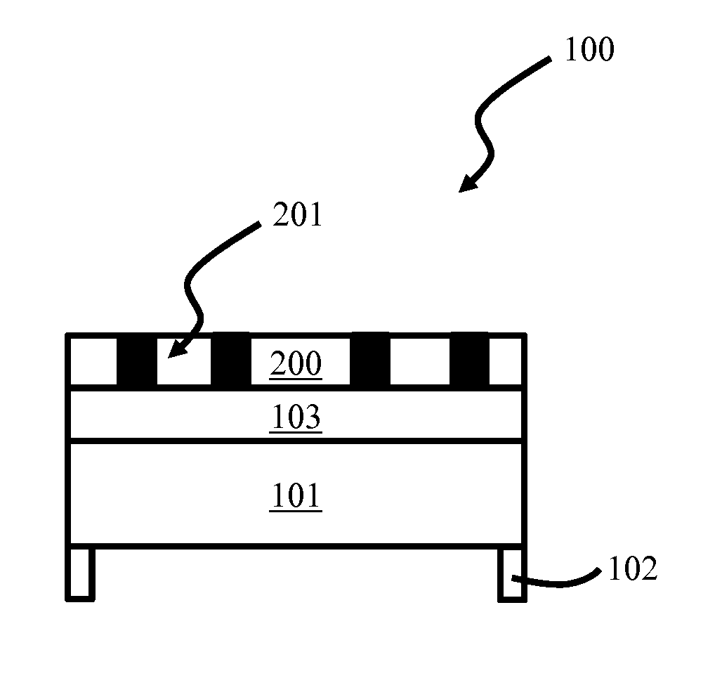
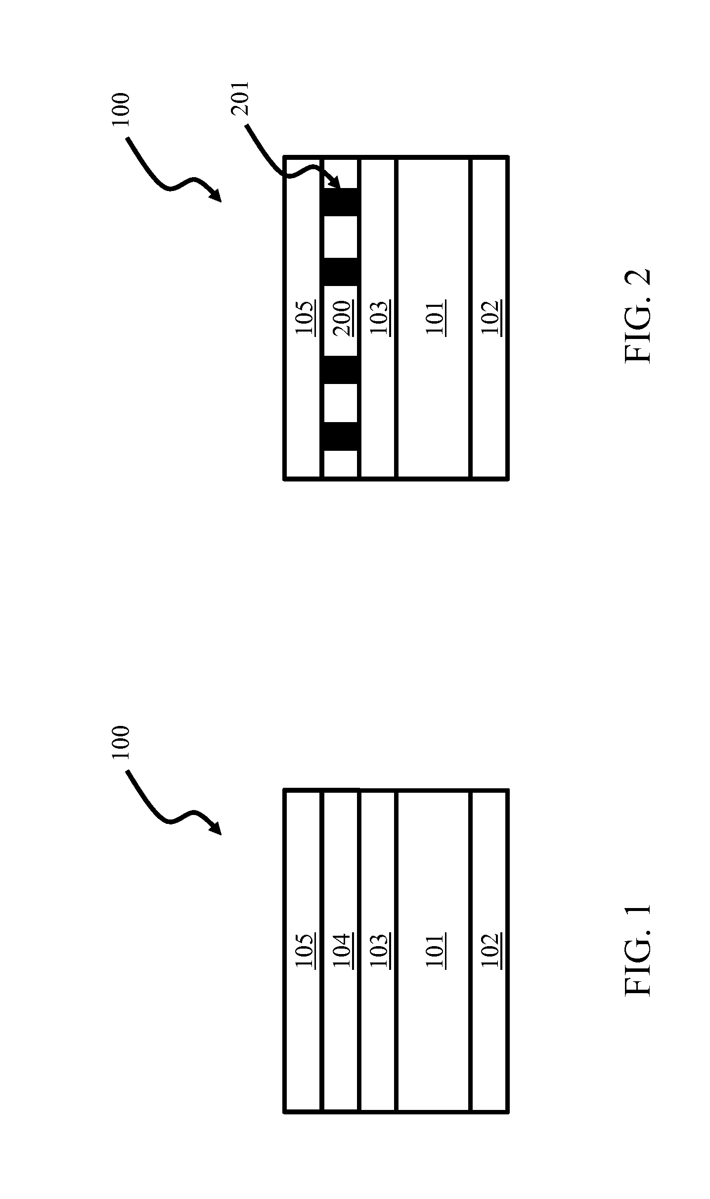
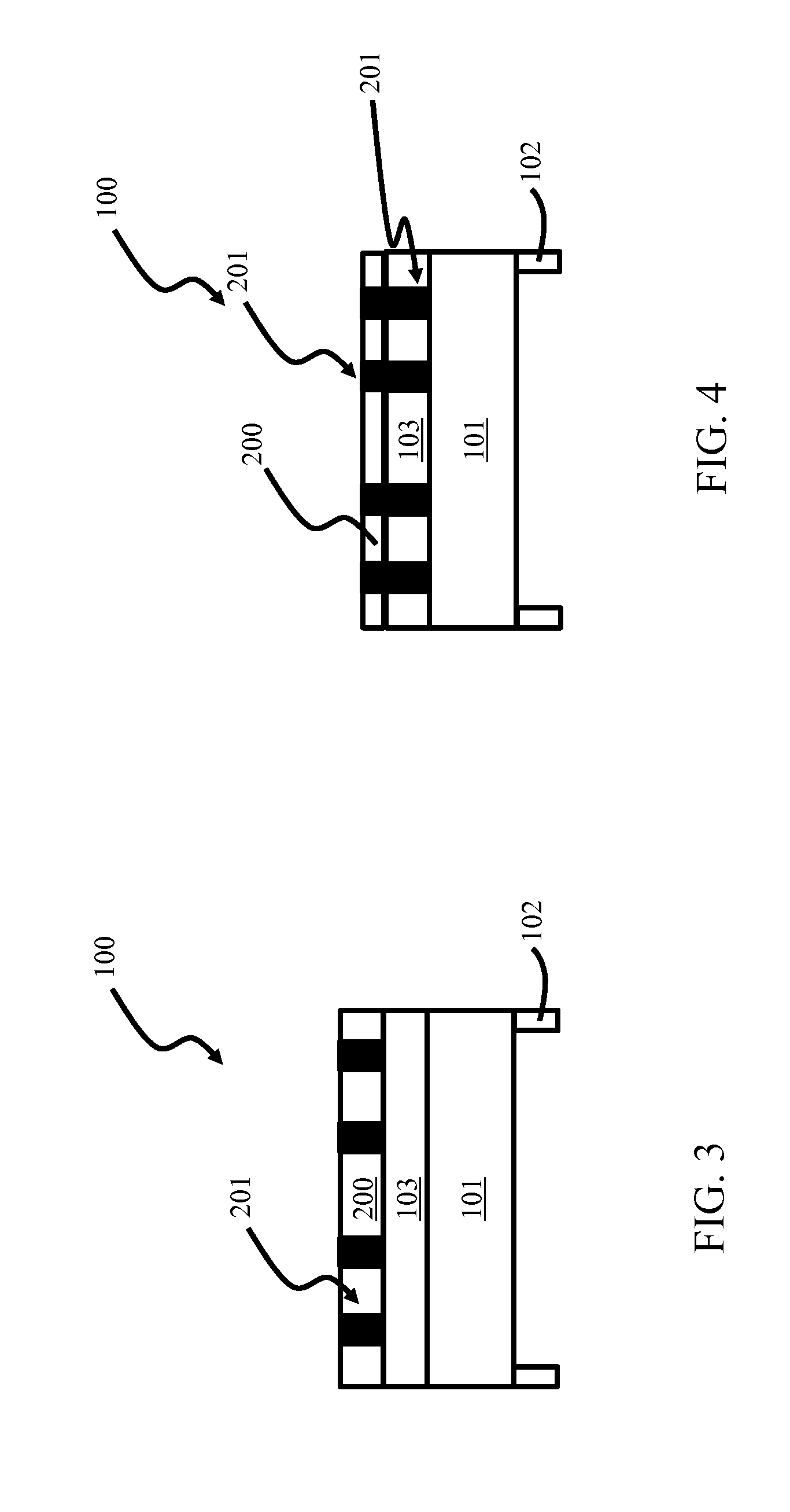
[0060]FIGS. 1-5 are schematic representations of a first example of an SiN membrane manufacturing process. In FIG. 1, the substrate 100 included Si layer 101, SiN layer 102, SiN layer 103, amorphous silicon (a-Si) layer 104, and SiO2 layer 105. In this example, the SiN layer 102 and SiN layer 103 were both approximately 50 nm in thickness, the a-Si layer 104 was approximately 40 nm in thickness, and the SiO2 layer 105 was approximately 20 nm in thickness, though other dimensions are possible. The capping SiO2 layer keeps the a-Si layer from agglomerating / deforming during the thermal annealing step that forms the pnc-Si. In FIG. 2, a thermal process, such as a rapid thermal processing (RTP) step, has been performed. The a-Si layer 104 of FIG. 1 was converted to a pnc-Si layer 200 using this thermal process. The pnc-Si layer 200 contains pores 201 (illustrated in black). These pores 201 may be approximately 5 nm to 80 nm in dimension. While only four pores 201 are illustrated, this is...
example 2
[0064]FIGS. 6-8 are schematic representations of a second example of an SiN membrane manufacturing process. The example of FIGS. 6-8 may be combined with steps from Example 1 or may be a standalone process. This example may be referred to as a “lift-off” process. In FIG. 6, the pores 201 (illustrated in black) in the SiN layer 103 were formed using an RIE. The pnc-Si layer was completely removed from the surface of the SiN layer 103 during this RIE. A sacrificial SiO2 layer 300 was formed between the Si layer 101 and the SiN layer 103 prior to formation of the SiN layer 103.
[0065]A scaffold 301 was applied to the SiN layer 103 in FIG. 7. The scaffold 301 was SU-8 photoresist (3010 series manufactured by Microchem International), though other materials are possible. This scaffold 301 was formed by spin coating the SU-8 photoresist to a thickness of 10 μm on top of the membrane, patterning the SU-8 photoresist to form an 80% open scaffold using contact photolithography, and developing...
example 3
[0070]FIGS. 12-13 are STEM images of an SiN membrane and a pnc-Si mask. FIG. 12 illustrates a 40 nm thick pnc-Si film. The lighter areas in FIG. 12 are pores. FIG. 13 shows these pores transferred to a 50 nm thick SiN film using RIE of the pnc-Si mask of FIG. 12. The 40 nm pnc-Si film had an average pore diameter of approximately 38 nm and a porosity of approximately 6%. The SiN had an average pore diameter of approximately 61 nm and a porosity of approximately 30%.
PUM
 Abstract
Description
Claims
Application Information
 - R&D Engineer
- R&D Manager
- IP Professional
- Industry Leading Data Capabilities
- Powerful AI technology
- Patent DNA Extraction
Browse by: Latest US Patents, China's latest patents, Technical Efficacy Thesaurus, Application Domain, Technology Topic.
© 2024 PatSnap. All rights reserved.Legal|Privacy policy|Modern Slavery Act Transparency Statement|Sitemap