

Imaging device and focusing control method
a technology of focusing control and imaging device, which is applied in the field of imaging device and focusing control method, can solve the problems of low imaging quality, and achieve the effect of enhancing imaging quality and preventing focusing errors
- Summary
- Abstract
- Description
- Claims
- Application Information
AI Technical Summary
Benefits of technology
Problems solved by technology
Method used
Image

Examples
first modification example
[0144](First Modification Example of Array)
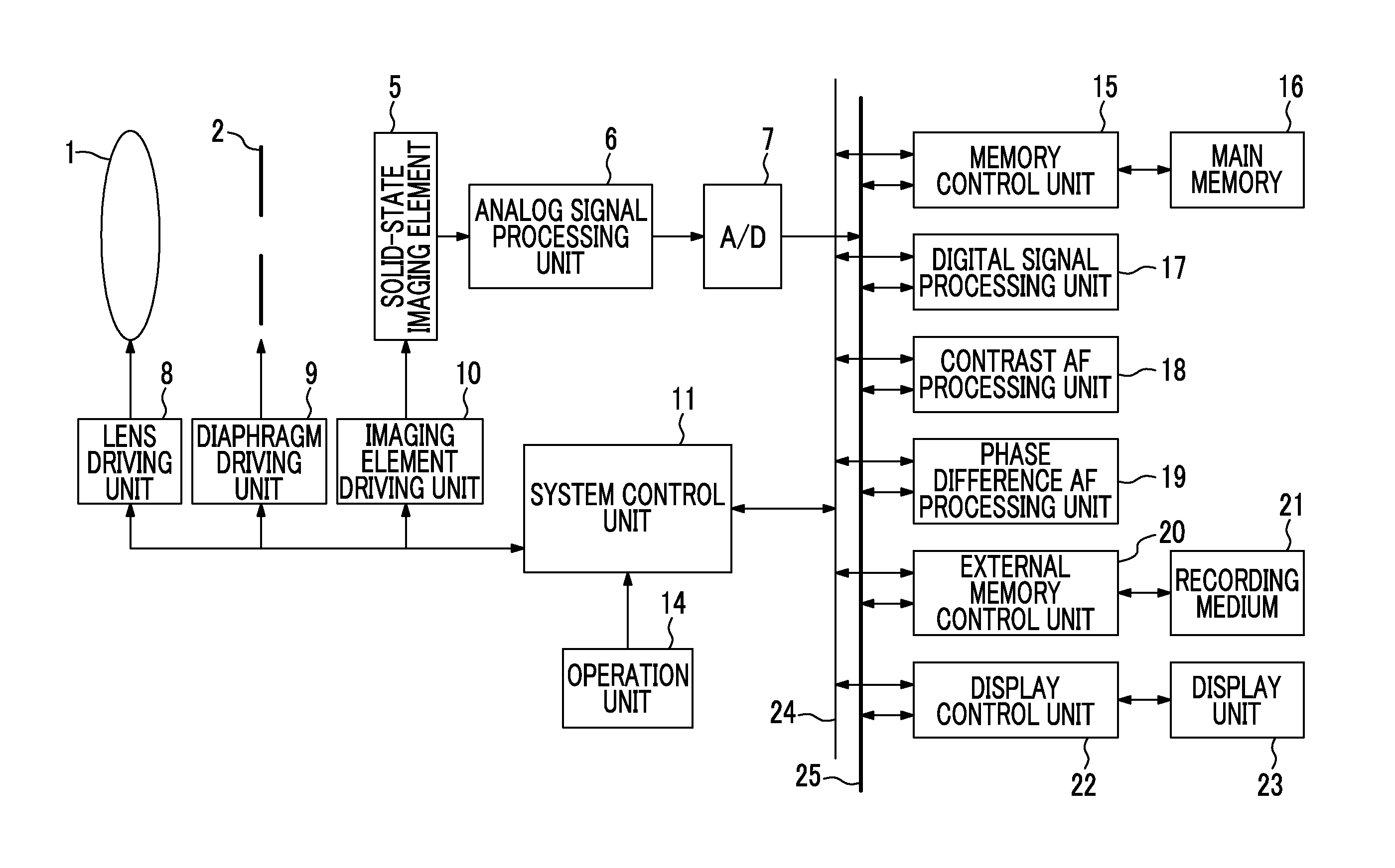
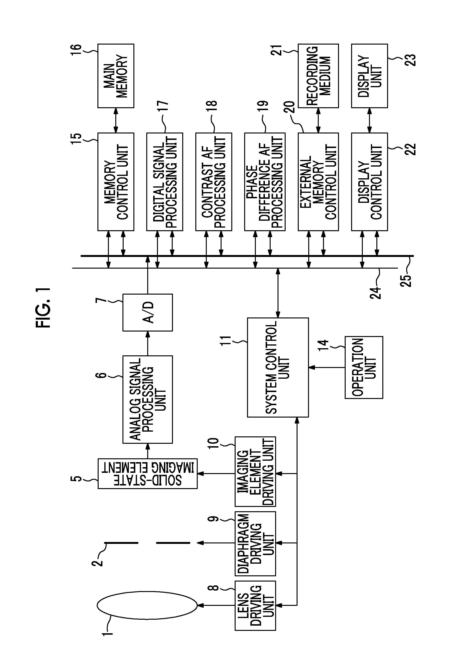
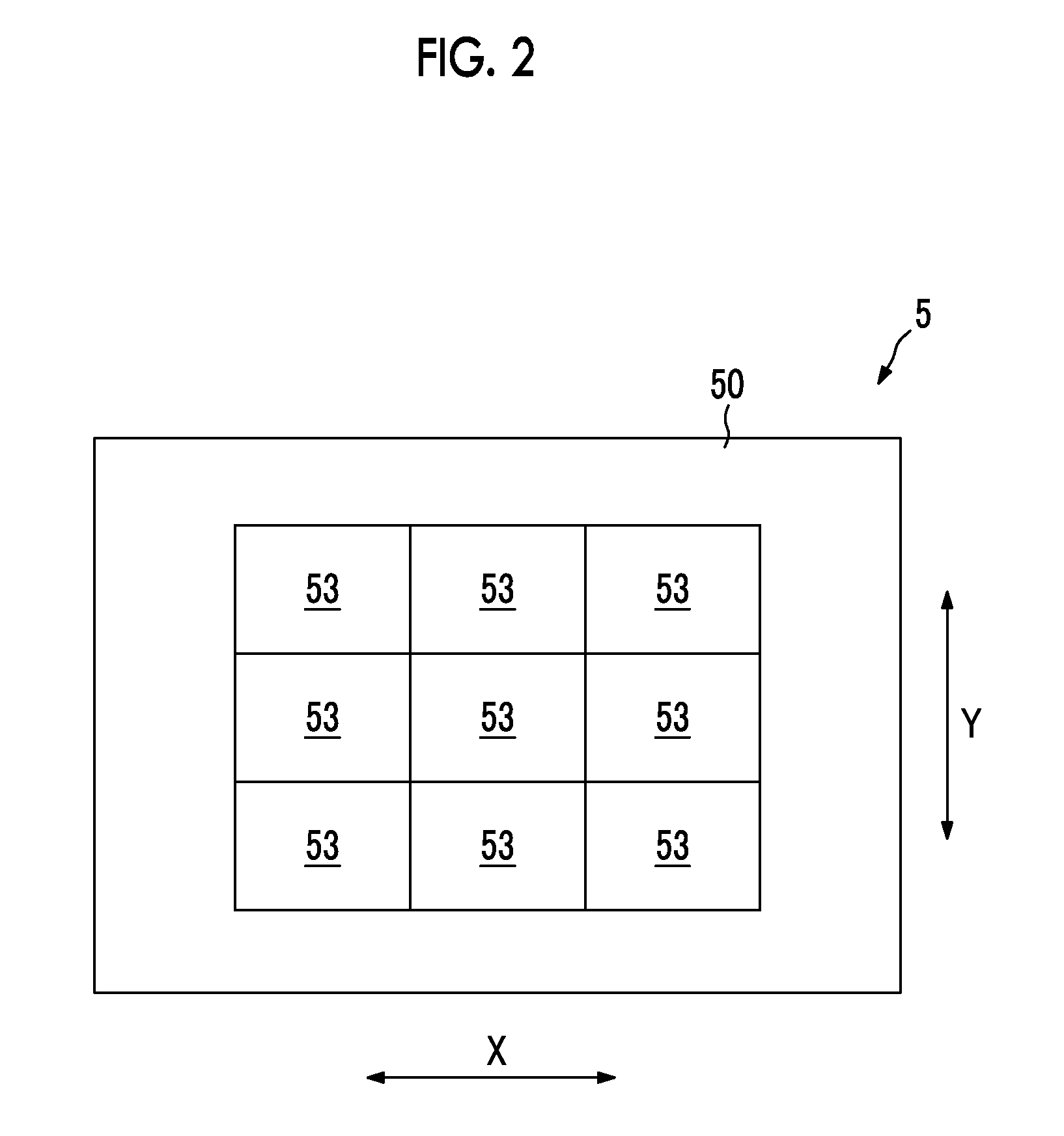
[0145]FIG. 9 is a diagram illustrating a modification example of the array of the phase difference detection pixels 52A and 52B which are positioned in the AF area 53 of the solid-state imaging element 5 shown in FIG. 1.
[0146]In the array example shown in FIG. 9, two phase difference pixel lines that include plural phase difference detection pixels 52A arranged in the row direction X, and two phase difference pixel lines that include plural phase difference detection pixels 52B arranged in the row direction X are provided in the AF area 53, and reliability determination is performed using the four phase difference pixel lines as one block. In the following description of FIG. 9, for ease of description, it is assumed that the upward direction and the downward direction represent a vertical direction in the figure.
[0147]In one block shown in FIG. 9, respective phase difference detection pixels included in phase difference pixel lines in odd-...
second modification example
[0153](Second Modification Example of Array)
[0154]FIG. 10 is a diagram illustrating a modification example of the array of the phase difference detection pixels 52A and 52B which are positioned in the AF area 53 of the solid-state imaging element 5 shown in FIG. 1.
[0155]In the array example shown in FIG. 10, two phase difference pixel lines that include plural phase difference detection pixels 52A arranged in the row direction X, and two phase difference pixel lines that include plural phase difference detection pixels 52B arranged in the row direction X are provided in the AF area 53, and reliability determination is performed using the four phase difference pixel lines as one block.
[0156]In one block shown in FIG. 10, each phase difference pixel included in phase difference pixel lines in the first row and the fourth row is the phase difference detection pixel 52A, and each phase difference pixel included in phase difference pixel lines in the second row and the third row is the p...
third modification example
[0161](Third Modification Example of Array)
[0162]FIG. 11 is a diagram illustrating a modification example of the array of the phase difference detection pixels 52A and 52B which are positioned at the AF area 53 of the solid-state imaging element 5 shown in FIG. 1.
[0163]In the array example shown in FIG. 11, two phase difference pixel lines that include plural phase difference detection pixels 52B arranged in the row direction X, and one phase difference pixel line that includes plural phase difference detection pixels 52A arranged in the row direction X are provided in the AF area 53, and reliability determination is performed using the three phase difference pixel lines as one block.
[0164]In the array example shown in FIG. 11, each phase difference detection pixel 52A disposed in an odd column among the phase difference detection pixels 52A in the phase difference pixel line in the second row in the block and each phase difference detection pixel 52B disposed at a one-pixel interva...
PUM
 Abstract
Description
Claims
Application Information