

Semiconductor manufacturing apparatus
- Summary
- Abstract
- Description
- Claims
- Application Information
AI Technical Summary
Benefits of technology
Problems solved by technology
Method used
Image

Examples
first embodiment
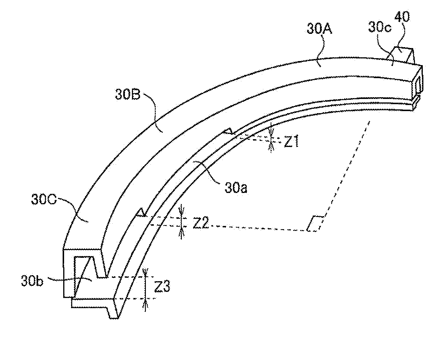
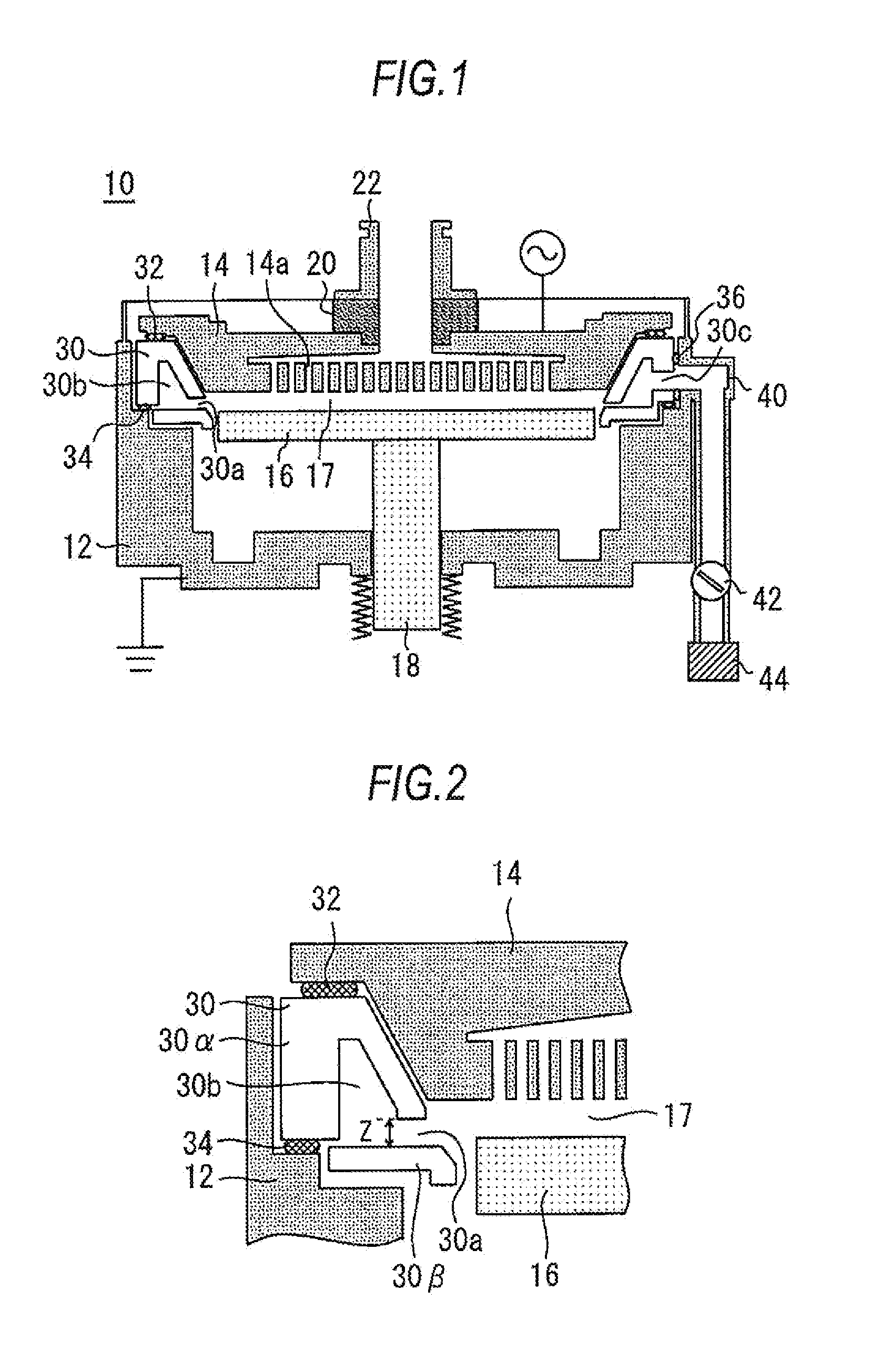
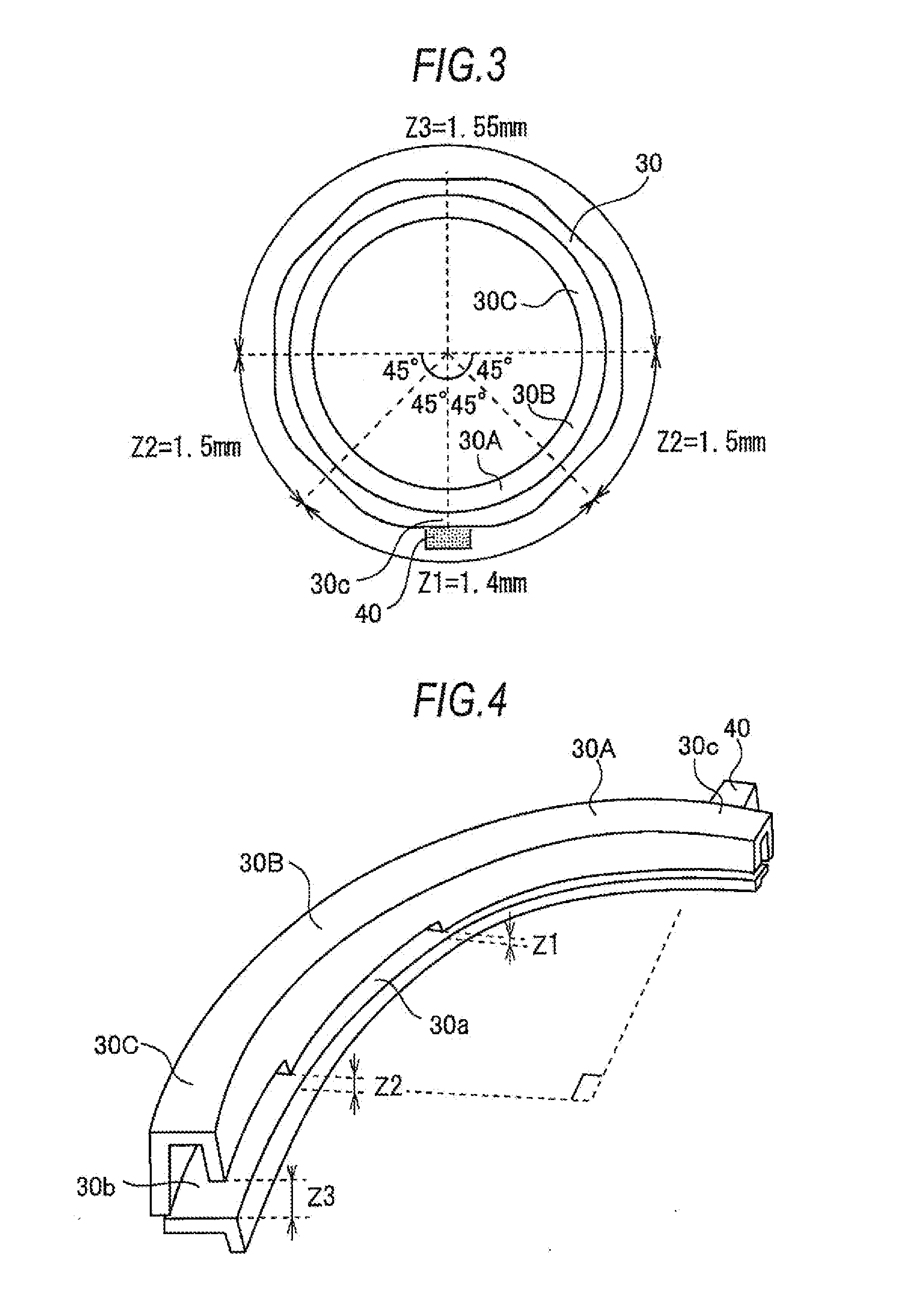
[0022]FIG. 1 is a sectional view of a semiconductor manufacturing apparatus 10 according to a first embodiment of the present invention. The semiconductor manufacturing apparatus 10 is constructed as a film forming apparatus with which plasma enhanced atomic layer deposition (PEALD) for example is performed on a substrate. The semiconductor manufacturing apparatus 10 comprises a chamber (reactor chamber) 12. An RF electrode 14 to which RF power is applied is provided in the chamber 12. Holes 14a are formed in the RF electrode 14.
[0023]A stage 16 is provided in the chamber 12 so as to be opposed to the RF electrode 14. The stage 16 is a susceptor supported on a slide shaft 18. The RF electrode 14 and the stage 16 form a parallel flat plate structure.
[0024]A gas supply part 22 is connected to the RF electrode 14, with an insulating part 20 interposed therebetween. The gas supply part 22 is a part through which a material gas is supplied to a space between the RF electrode 14 and the s...
second embodiment
[0039]FIG. 5 is a perspective view of a portion of an exhaust duct 50 of the semiconductor manufacturing apparatus according to the second embodiment of the present invention. The extent Z of the slit 30a in the vertical direction is increased steplessly with increase in distance from the exhaust port 30c. Accordingly, the extent Z of the slit 30a in the vertical direction is minimized in its portion at which the exhaust port 30c is formed, and is maximized in its portion farthermost from the exhaust port 30c.
[0040]With this slit shape, the flow of gas from a position in the processing space close to the exhaust port 30c to the annular passage 30b is suppressed and the flow of gas from a position in the processing space remote from the exhaust port 30c is promoted, thus improving the uniformity of the gas flow rate at the stage edge.
[0041]In the meantime, in the exhaust duct 50 according to the second embodiment, the gas flow rate is higher at a position P1 in the slit 30a reached ...
third embodiment
[0044]FIG. 6 is a plan view of the lower part 30β of the exhaust duct of the semiconductor manufacturing apparatus according to the third embodiment of the present invention. In this exhaust duct, portions of the slit are blocked with a plurality of obstacles. FIG. 6 illustrates the lower part 30β and a plurality of obstacles. As the plurality of obstacles, three obstacles 50a, eleven obstacles 50b and three obstacles 50c are provided. The obstacles 50b are formed near the exhaust port 30c. The obstacles 50a and the obstacles 50c are provided at positions between which the obstacles 50b are located.
[0045]Each of the three obstacles 50a and the three obstacles 50c is an obstacle of a comparatively small width. The eleven obstacles are each an obstacle of a width about twice that of the obstacles 50a and 50c. The obstacles 50b are provided at a density twice the density at which the obstacles 50a and 50c are provided. Consequently, the plurality of obstacles block portions of the slit...
PUM
| Property | Measurement | Unit |
|---|---|---|
| Density | aaaaa | aaaaa |
| Distance | aaaaa | aaaaa |
| Circumference | aaaaa | aaaaa |
Abstract
Description
Claims
Application Information