
Method wherein test cells and dummy cells are included into a layout of an integrated circuit

a technology of integrated circuit and layout, which is applied in the direction of electric digital data processing, total factory control, instruments, etc., can solve the problems of small space available, reducing the sensitivity of the photolithography process with respect to variations in photolithography parameters, and the possibility of inclusion of test cells into the middle of line (mol) layer of the integrated circuit may be even more limited

Inactive Publication Date: 2016-11-10
GLOBALFOUNDRIES INC
View PDF1 Cites 77 Cited by
  • Summary
  • Abstract
  • Description
  • Claims
  • Application Information

AI Technical Summary

Benefits of technology

The invention describes a method for designing an integrated circuit layout that can accommodate test cells and dummy cells. The method involves dividing the layout into tiles, with each tile containing available space for inclusion of one or more test cells or dummy cells. The method takes into account space availability information and optimizes the layout to make efficient use of available space. The technical effect of this invention is that it enables efficient and effective placement of test cells and dummy cells in an integrated circuit layout.

Problems solved by technology

However, the presence of SRAFs may reduce a sensitivity of the photolithography process with respect to variations of parameters of the photolithography process, which may include, in particular, a focus of the projection and a dose of the radiation used for projecting the reticle to the photoresist.
In advanced technology nodes, for example in the 28 nm technology node or below, only relatively small amounts of space may be available between circuit features, which may be as small as 9×3.5 μm2 or 4×2 μm2 in front-end-of-line (FEOL) layers of the integrated circuit, and 4×4 μm2 in back-end-of-line (BEOL) layers, and the possibilities for inclusion of test cells into middle-of-line (MOL) layers of the integrated circuit may be even more limited.

Method used


Image

  • Method wherein test cells and dummy cells are included into a layout of an integrated circuit
  • Method wherein test cells and dummy cells are included into a layout of an integrated circuit
  • Method wherein test cells and dummy cells are included into a layout of an integrated circuit

Examples


Embodiment Construction

[0037]Various illustrative embodiments of the invention are described below. In the interest of clarity, not all features of an actual implementation are described in this specification. It will of course be appreciated that in the development of any such actual embodiment, numerous implementation-specific decisions must be made to achieve the developers' specific goals, such as compliance with system-related and business-related constraints, which will vary from one implementation to another. Moreover, it will be appreciated that such a development effort might be complex and time-consuming, but would nevertheless be a routine undertaking for those of ordinary skill in the art having the benefit of this disclosure.

[0038]The present disclosure will now be described with reference to the attached figures. Various structures, systems and devices are schematically depicted in the drawings for purposes of explanation only and so as to not obscure the present disclosure with details whic...


PUM


Abstract

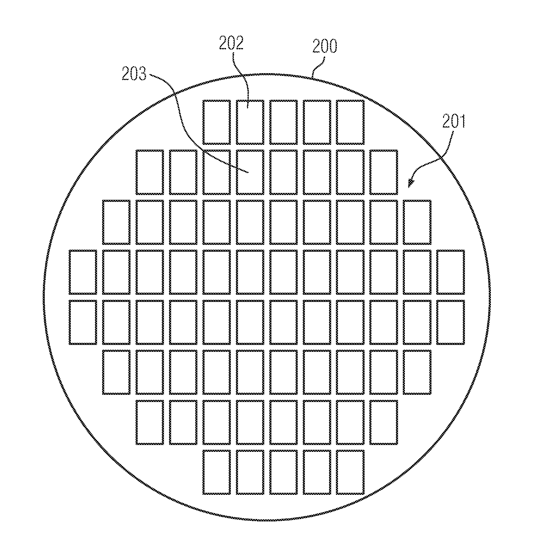
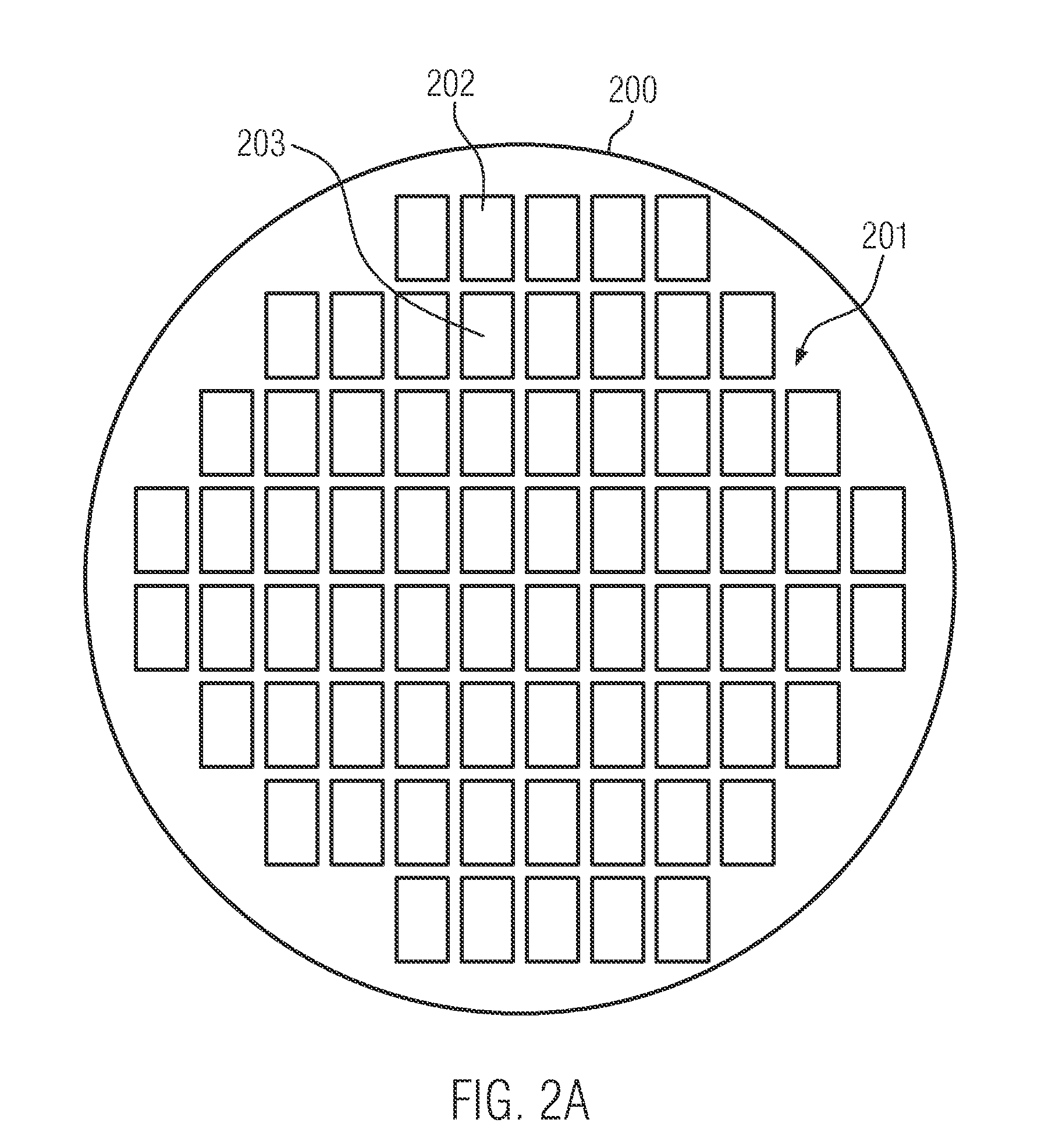
A method includes receiving a layout of an integrated circuit that includes a plurality of layers, one of the layers is selected and one or more tile number values are provided. A die area of the integrated circuit is partitioned into a plurality of tiles on the basis of the tile number values. It is determined, on the basis of the layout, if a portion of the selected one of the layers in the tile has an available space for inclusion of a test cell or a dummy cell, and a label indicative of a result is assigned to the tile. It is determined, on the basis of the labels assigned, if one or more space availability criteria are fulfilled and, if fulfilled, the labels are used for placing at least one of one or more test cells and one or more dummy cells in the layout.

Description

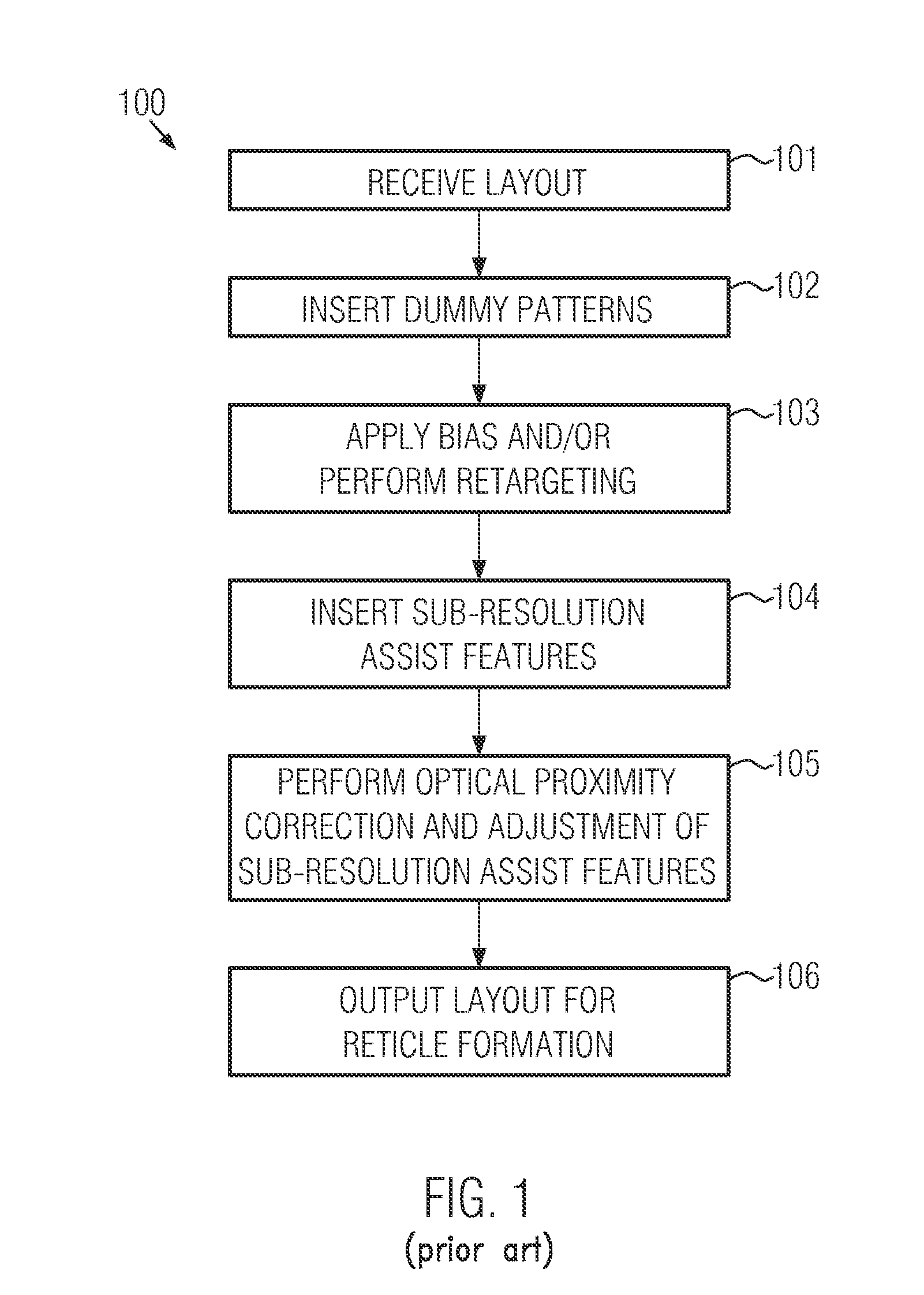
BACKGROUND OF THE INVENTION[0001]1. Field of the Invention[0002]Generally, the present disclosure relates to the manufacturing of integrated circuits and, in particular, to the provision of layouts of integrated circuits including test cells.[0003]2. Description of the Related Art[0004]Integrated circuits typically include a large number of circuit elements which include, in particular, field effect transistors. The circuit elements in an integrated circuit may be electrically connected by means of electrically conductive metal lines formed in a dielectric material, for example, by means of damascene techniques. The electrically conductive metal lines may be provided in a plurality of metal layers that are arranged above each other over a substrate in and on which the circuit elements are formed. Metal lines in different metal layers may be electrically connected with each other by means of contact vias that are filled with metal and are provided in via layers that are arranged betw...

Claims


Application Information

Patent Timeline
Patent Type & Authority Applications(United States)
IPC IPC(8): G06F17/50
CPCG06F2217/12G06F17/5072G01R31/26H01L22/14H01L23/544G06F30/333G06F2119/18G06F30/392Y02P90/02G06F30/398G06F2111/04
Inventor UEBERREITER, GUIDOACKMANN, PAULNING, GUOXIANGFENG, JUI-HSUANLIM, CHIN TEONG
Owner GLOBALFOUNDRIES INC
Learn More