Array substrate and driving method thereof, display panel and display device

a technology applied in the field of array substrate and driving method thereof, display panel and display device, can solve the problems of inability to reduce the size of each sub-pixel unlimitedly, inability to fabricate more pixel circuits accordingly, and difficulty in fabricating high-resolution display panel, etc., to reduce production cost and process pressure, and reduce the number of pixel circuits.

Active Publication Date: 2016-11-17
BOE TECH GRP CO LTD
View PDF22 Cites 14 Cited by
  • Summary
  • Abstract
  • Description
  • Claims
  • Application Information

AI Technical Summary

Benefits of technology

[0014]In the array substrate of the embodiments of the invention, the first sub-pixel and the second sub-pixel in each sub-pixel unit are driven by the same pixel circuit, and compared to the prior art in which it is required to drive the first sub-pixel and the second sub-pixel in each sub-pixel unit using two pixel circuits, respectively, the number of the pixel circuits required in the entire array substrate is reduced, thus decreasing production cost and process pressure. At the same time, since the number of the pixel circuits is reduced, more sub-pixel units can be formed per unit area on the array substrate, thus effectively increasing resolution of the array substrate.

Problems solved by technology

However, due to process constraints, apparently, the size of each sub-pixel cannot be decreased unlimitedly.
However, as understood by persons skilled in the art, each pixel unit requires to be driven by one pixel circuit, and due to the limitation on the size of the display panel, although more pixel units may be fabricated, there is no way to fabricate more pixel circuits accordingly, thus it is still very difficult to fabricate a high resolution display panel.

Method used


Image

  • Array substrate and driving method thereof, display panel and display device
  • Array substrate and driving method thereof, display panel and display device
  • Array substrate and driving method thereof, display panel and display device

Examples


Embodiment Construction

[0019]In order to make persons skilled in the art better understand the technical solutions of the invention, the invention will be further described in detail below in connection with the drawings and the implementations.

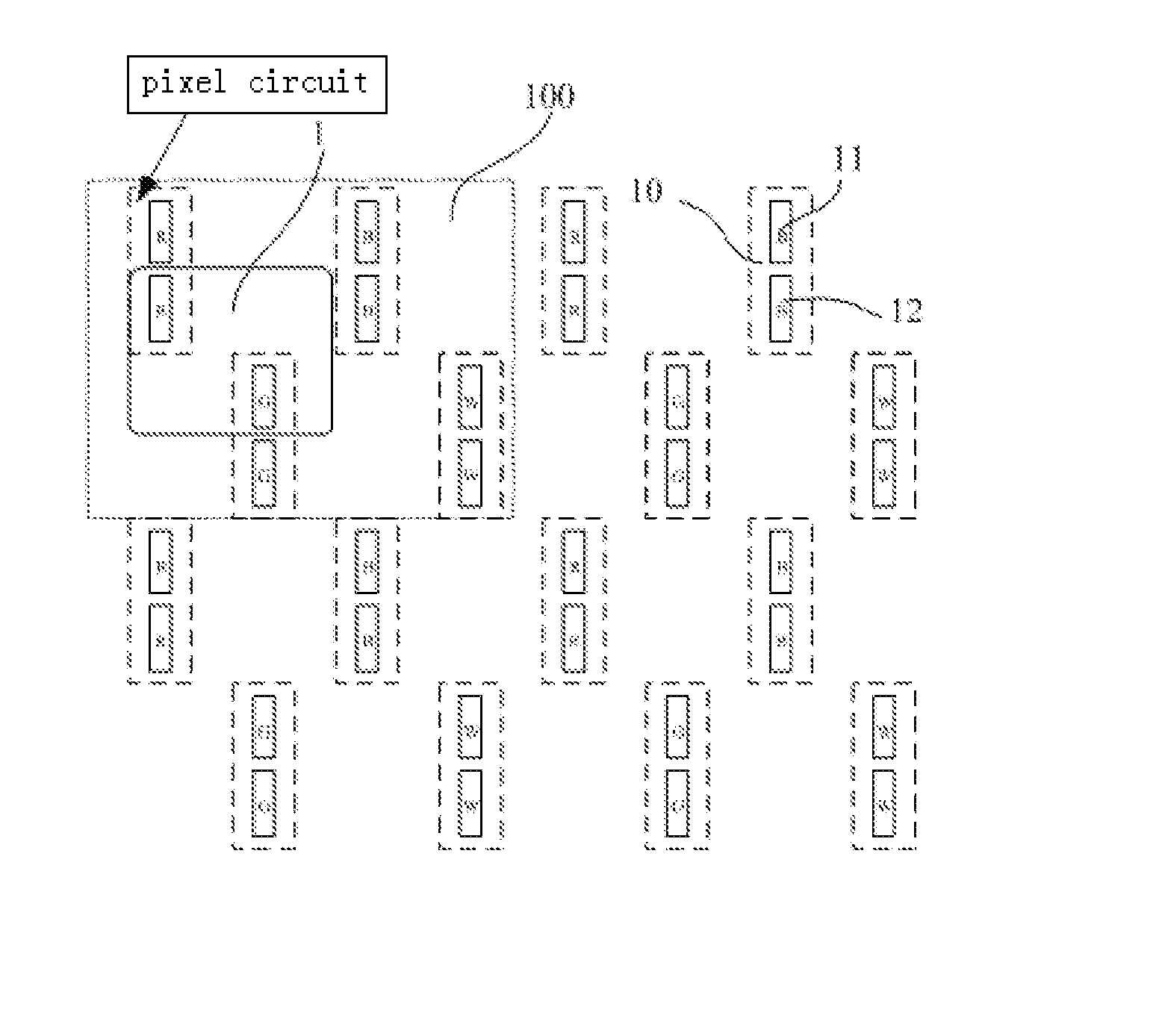
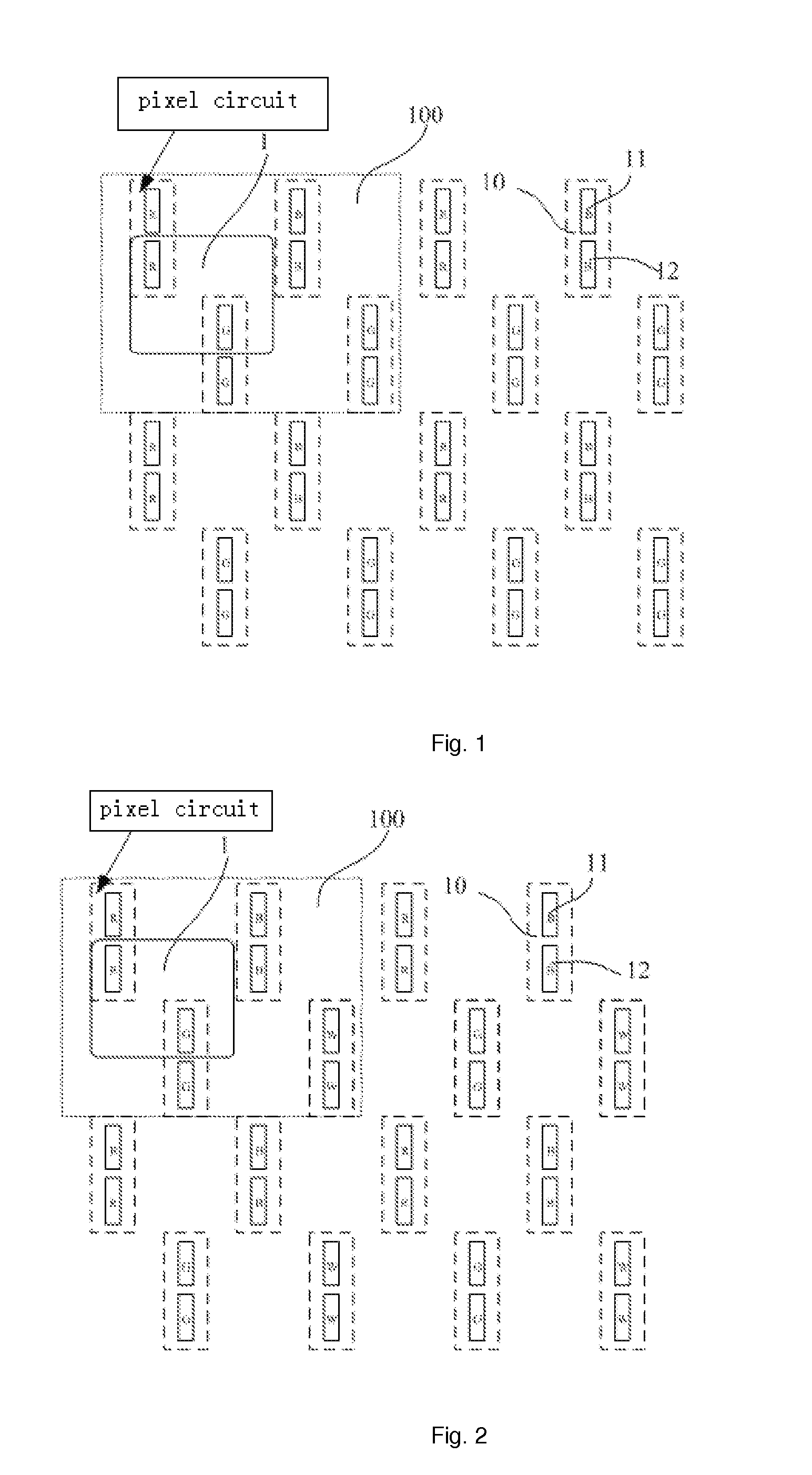
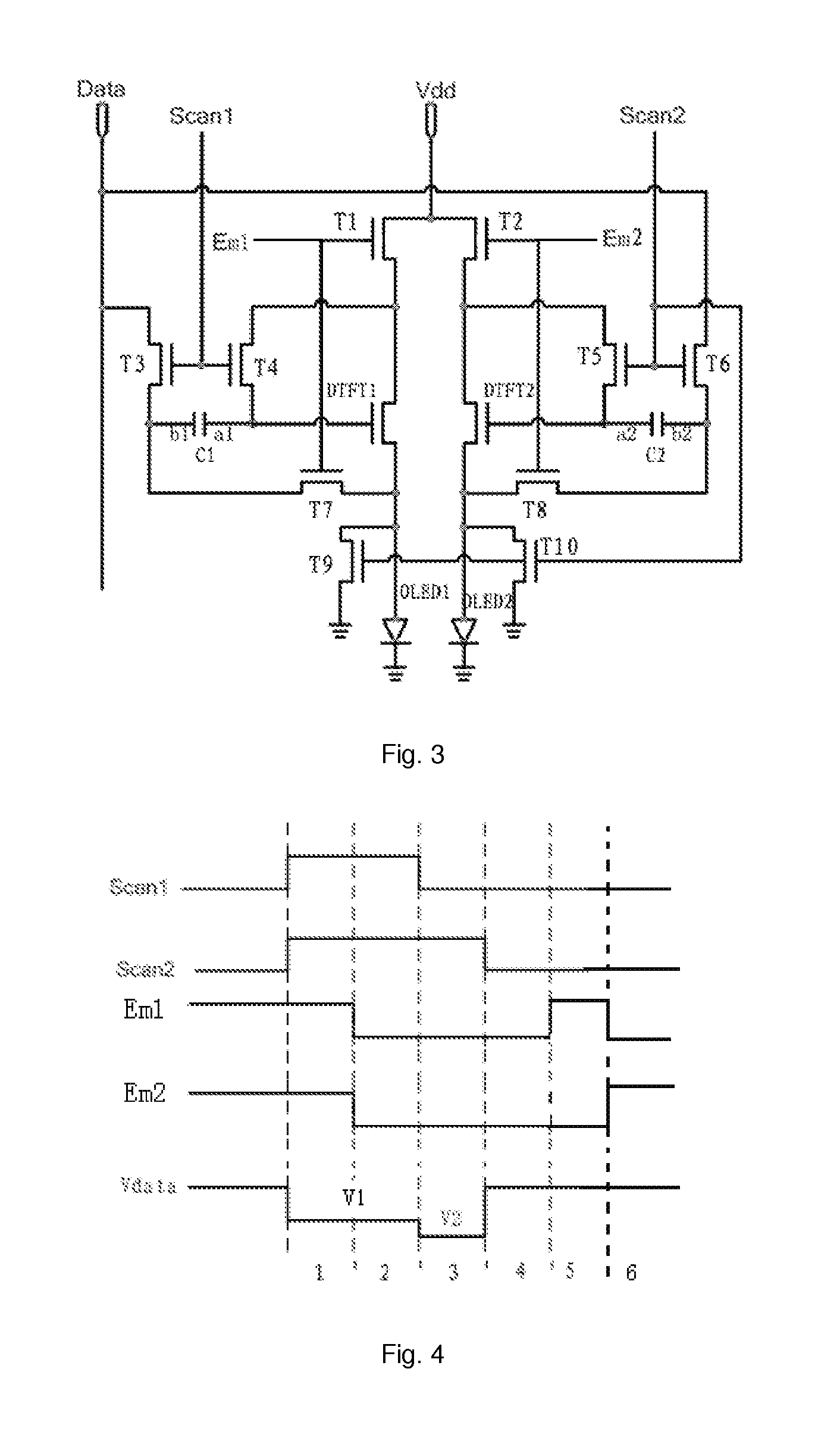
[0020]In connection with FIGS. 1 and 2, the embodiment of the invention provides an array substrate, which comprises a plurality of circulating units 100, each circulating unit 100 consists of four sub-pixel units 10 located in four columns and two rows, sub-pixel units 10 in every two adjacent columns are located in different rows and have different colors, and sub-pixel units 10 in at least one row have different colors. The array substrate further comprises a plurality of pixel circuits, each sub-pixel unit 10 is connected to one pixel circuit, each sub-pixel unit 10 comprises a first sub-pixel 11 and a second sub-pixel 12 located in the same column and having the same color. Each pixel circuit is configured to drive the first sub-pixel 11 when a first frame pic...


PUM


Abstract

The invention provides an array substrate and a driving method thereof, a display panel and a display device. The array substrate comprises a plurality of circulating units and a plurality of pixel circuits. Each circulating unit consists of four sub-pixel units located in four columns and two rows, sub-pixel units in any two adjacent columns are located in different rows and have different colors, and sub-pixel units in at least one row have different colors. Each sub-pixel unit is connected to one pixel circuit, and each sub-pixel unit comprises a first sub-pixel and a second sub-pixel located in the same column and having the same color. The pixel circuit is configured to drive the first sub-pixel when a first frame picture is displayed, and to drive the second sub-pixel when a second frame picture is displayed.

Description

TECHNICAL FIELD[0001]The invention relates to the field of display technology, and in particular to an array substrate and a driving method thereof, a display panel and a display device.BACKGROUND[0002]With the development of technology, the resolution of a display panel is higher and higher. That is, the number of pixels in the unit area is increasing, which requires that size of each sub-pixel is becoming smaller and smaller. However, due to process constraints, apparently, the size of each sub-pixel cannot be decreased unlimitedly.[0003]In order to improve the display effect under a given size of the sub-pixel, a display device in the Pentile mode is proposed. In the display device in the Pentile mode, sub-pixels of certain colors (such as red sub-pixels and blue sub-pixels) are decreased in number while sub-pixels of different colors in the display device are virtually considered to be in different “layers”, and each layer is divided into a plurality of sampling regions, samplin...

Claims


Application Information

Patent Timeline
Patent Type & Authority Applications(United States)
IPC IPC(8): G09G3/20G09G3/3208
CPCG09G3/2074G09G3/2003G09G3/3233G09G2300/0804G09G2300/0814G09G2300/0861G09G2310/0251G09G2300/0443G09G2300/0452G09G2300/0465G09G2300/0852G09G2340/0457G02F1/133G06F3/14G09G3/20G09G3/32G09G3/36G09G5/00G09G2300/0426
Inventor LEE, CHUNGCHUNDUAN, LIYELI, YANZHAOWU, CHUNWEIPARK, HANJUN
Owner BOE TECH GRP CO LTD
Why Eureka
Try Eureka