Semiconductor light emitting structure and manufacturing method thereof

Inactive Publication Date: 2016-12-01
LEXTAR ELECTRONICS CORP
View PDF7 Cites 2 Cited by
  • Summary
  • Abstract
  • Description
  • Claims
  • Application Information

AI Technical Summary

Benefits of technology

[0007]The invention is directed to a semiconductor light emitting structure and a manufacturing method thereof, in which a stepped electrode is formed within the ep

Problems solved by technology

Therefore, a part of the light will be absorbed and cannot be completely extracted

Method used


Image

  • Semiconductor light emitting structure and manufacturing method thereof
  • Semiconductor light emitting structure and manufacturing method thereof
  • Semiconductor light emitting structure and manufacturing method thereof

Examples


Example

[0017]A number of embodiments are disclosed below for elaborating the invention. However, the embodiments of the invention are for detailed descriptions only, not for limiting the scope of protection of the invention.

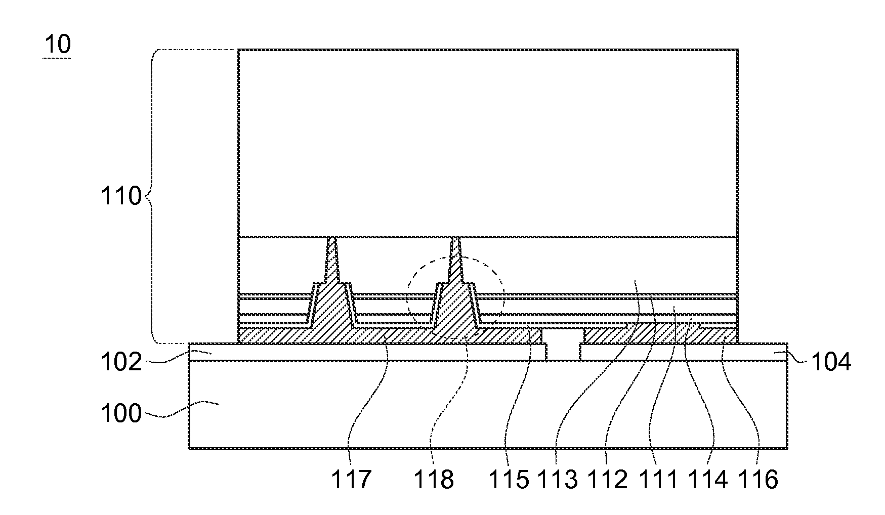
[0018]Referring to FIG. 1, a cross-sectional view of a semiconductor flip-chip package structure 10 according to an embodiment is shown.

[0019]In one embodiment, the semiconductor flip-chip package structure 10 includes a carrier 100 and a light emitting unit 110. The light emitting unit 110 is disposed on the carrier 100, and the light emitting unit 110 has a P-type electrode 116 and an N-type electrode 117. The P-type electrode 116 is electrically connected to the positive electrode 104 of the carrier 100, and the N-type electrode 117 is electrically connected to the negative electrode 102 of the carrier 100 for transmitting and diffusing a current to the light emitting unit 110, such that electrons and holes in the light emitting unit 110 being driven by a voltage are...


PUM


Abstract

A semiconductor light emitting structure and a manufacturing method thereof are provided. The semiconductor light emitting structure includes a substrate, an epitaxial layer and a stepped electrode. The substrate has a first surface and a second surface opposite to the first surface. The epitaxial layer is formed by a first semiconductor layer, an active layer and a second semiconductor layer which are stacked on the first surface in sequence. The stepped electrode is formed within the epitaxial layer, and includes a main body portion, a step level and a reflection electrode portion extended towards the first surface from the step level. The main body portion at least passes through the second semiconductor layer and the active layer. The reflection electrode portion is extended into the first semiconductor layer from the main body portion.

Description

[0001]This application claims the benefit of Taiwan application Ser. No. 104116626, filed May 25, 2015, the subject matter of which is incorporated herein by reference.BACKGROUND OF THE INVENTION[0002]1. Field of the Invention[0003]The invention relates in general to a light emitting structure, and more particularly to a semiconductor light emitting structure with stepped electrode and a manufacturing method thereof.[0004]2. Description of the Related Art[0005]Light-emitting diode (LED) emits a light by converting an electric energy into an optical energy. After a current is applied to the LED, the current is diffused and infused to an epitaxial layer of the LED, such that electrons and holes are combined and release energy in the form of a light. The LED has the advantages of long lifespan, power saving and small volume. Along with the development of multicolor domains and high brightness in recent years, the LED has been widely used in the field of white light illumination to repl...

Claims


Application Information

Patent Timeline
IPC IPC(8): H01L33/40H01L33/38
CPCH01L33/405H01L2933/0033H01L2933/0016H01L33/38H01L33/382
Inventor CHEN, CHENG-HUNGLIN, CHAO-HSIEN
Owner LEXTAR ELECTRONICS CORP
Why Eureka
Try Eureka