Light emitting diode package and method of manufacturing the same

a technology of light-emitting diodes and packaging, which is applied in the direction of basic electric elements, electrical equipment, semiconductor devices, etc., can solve the problems of increasing material costs and total manufacturing costs, and achieve the effect of reducing optical loss and uniform output luminan

Active Publication Date: 2016-12-22
SAMSUNG ELECTRONICS CO LTD
View PDF6 Cites 10 Cited by
  • Summary
  • Abstract
  • Description
  • Claims
  • Application Information

AI Technical Summary

Benefits of technology

The patent text describes a smaller LED package that can reduce optical loss and create consistent lighting. The patent also describes a method for making this LED package. This technology can improve the performance of LED devices.

Problems solved by technology

Since the LED package needs not only an additional substrate but to also have a relatively large package size, the cost of materials may increase.
Also, the total manufacturing cost may increase due to an additional packaging process.

Method used


Image

  • Light emitting diode package and method of manufacturing the same
  • Light emitting diode package and method of manufacturing the same
  • Light emitting diode package and method of manufacturing the same

Examples


Embodiment Construction

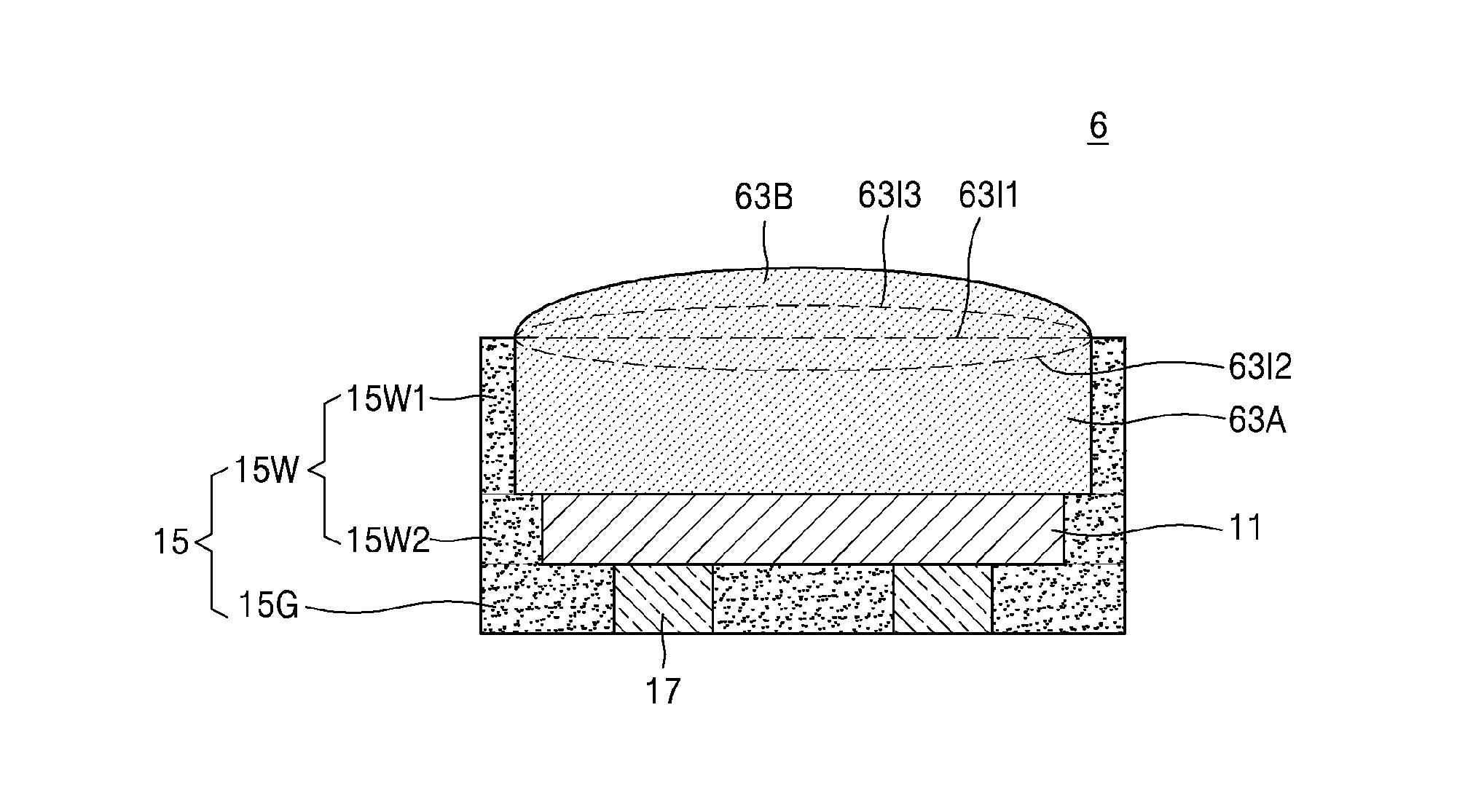
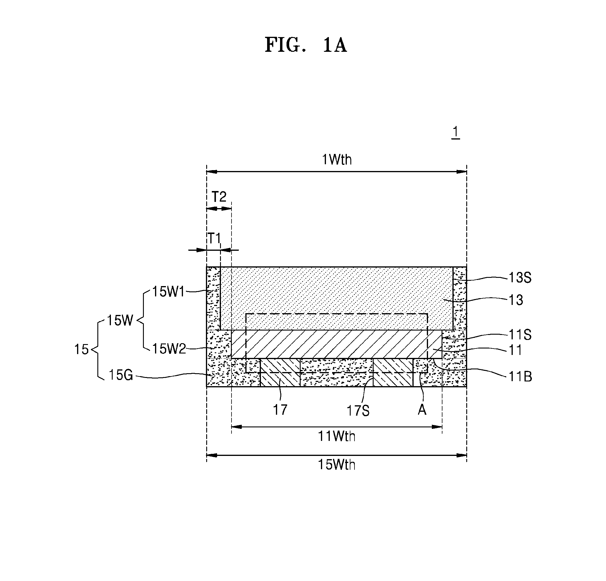
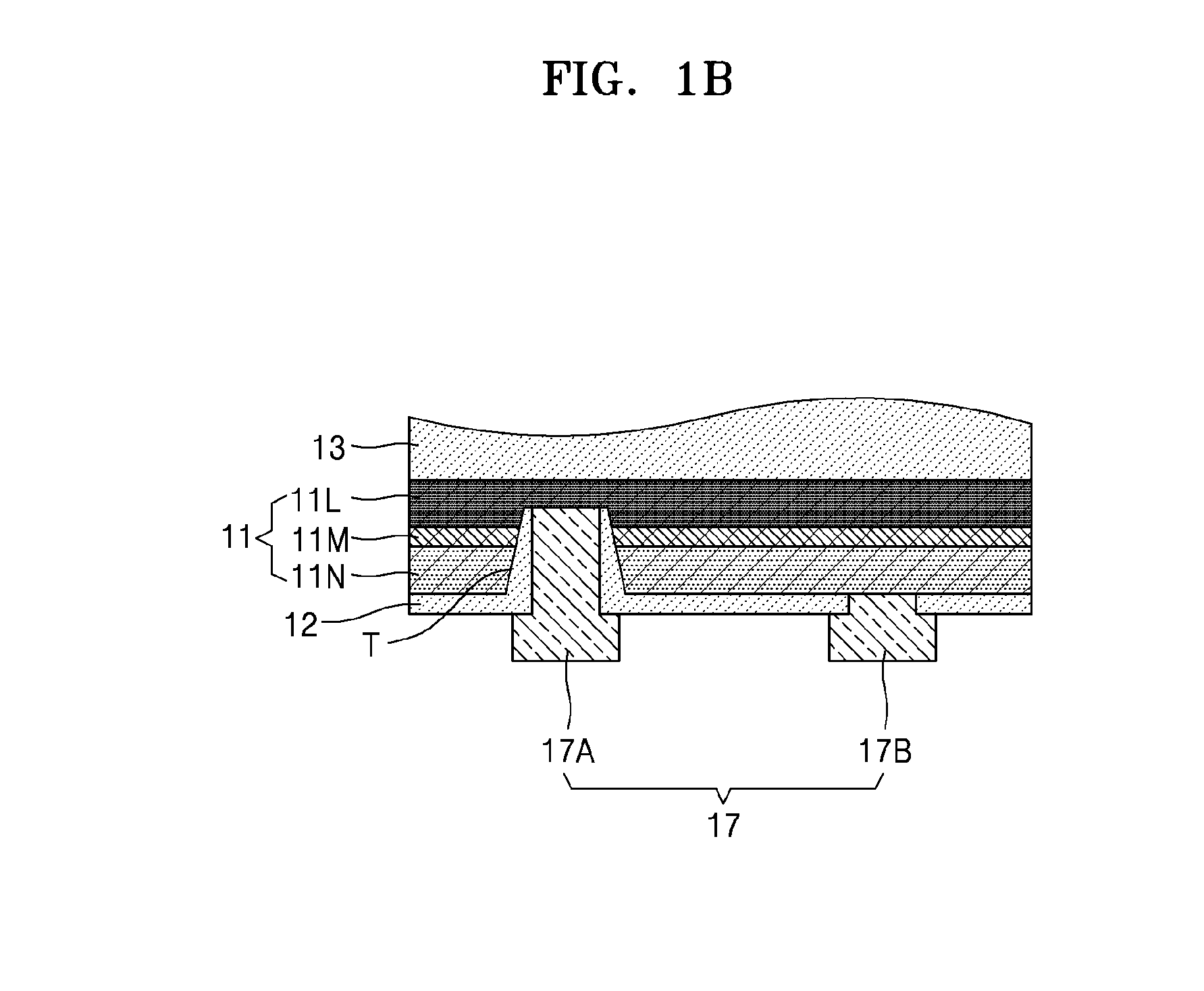
[0043]The inventive concepts now will be described more fully hereinafter with reference to the accompanying drawings, in which elements of the inventive concepts are shown.

[0044]The inventive concepts may, however, be embodied in many different forms and should not be construed as limited to the example embodiments set forth herein. Rather, these embodiments are provided so that this disclosure will be thorough and complete, and will fully convey the scope of the inventive concepts to one of ordinary skill in the art.

[0045]It will be understood that when an element is referred to as being “on” another element, it can be directly on the other element, or intervening elements may also be present therebetween. Likewise, it will be understood that when an element is referred to as being “connected” to another element, it may be “directly connected” to the other element or intervening elements may be present therebetween. Structures or sizes of elements in the drawings are exaggerated f...


PUM


Abstract

A light-emitting diode (LED) package includes a light-emitting structure, a transmissive material layer on the light-emitting structure, and a support structure covering at least a portion of a side surface of the transmissive material layer, a side surface of the light-emitting structure, and at least a portion of a bottom surface of the light-emitting structure.

Description

CROSS-REFERENCE TO RELATED APPLICATION[0001]This application claims the benefit of Korean Patent Application No. 10-2015-0087586, filed on Jun. 19, 2015, in the Korean Intellectual Property Office, the disclosure of which is incorporated herein in its entirety by reference.BACKGROUND[0002]1. Field[0003]Some example embodiments of the inventive concepts relate to a light-emitting diode (LED) package and / or a method of manufacturing the same, for example, to a chip-scale LED package and / or a method of manufacturing the same.[0004]2. Description of the Related Art[0005]In general, an LED package includes a chip mounted in a package including a lead frame substrate. Since the LED package needs not only an additional substrate but to also have a relatively large package size, the cost of materials may increase. Also, the total manufacturing cost may increase due to an additional packaging process.[0006]A chip-scale package (CSP), which is a package manufactured on a wafer level, may be e...

Claims


Application Information

Patent Timeline
Patent Type & Authority Applications(United States)
IPC IPC(8): H01L33/58H01L33/50H01L33/48H01L33/60H01L33/54H01L33/62
CPCH01L33/58H01L33/54H01L33/62H01L33/486H01L33/60H01L33/505H01L33/0075H01L2933/005H01L2933/0058H01L2933/0066H01L33/0095H01L33/0079H01L33/32H01L2933/0041H01L2224/96
Inventor CHO, HYUK-JINLEE, DONG-HOON
Owner SAMSUNG ELECTRONICS CO LTD
Why Eureka
Try Eureka