Fan-out package structure including antenna

a technology of semiconductor package and antenna, which is applied in the direction of semiconductor device details, semiconductor/solid-state devices, electrical devices, etc., can solve the problems of poor smt process control, delamination between the antenna component and the underlying package, and the difficulty of reducing the package size, etc., to achieve the effect of reducing reliability, yield and throughput of the semiconductor package structur

Inactive Publication Date: 2017-02-09
MEDIATEK INC
View PDF6 Cites 84 Cited by
  • Summary
  • Abstract
  • Description
  • Claims
  • Application Information

AI Technical Summary

Problems solved by technology

As a result, it is difficult to reduce the size of the package.
Moreover, in this case, since the antenna component is typically mounted on the package by a surface mount technology (SMT) process, poor SMT process control may induce delamination between the antenna component and the underlying package.
As a result, reliability, yield, and throughput of the semiconductor package structure are reduced.

Method used


Image

  • Fan-out package structure including antenna
  • Fan-out package structure including antenna
  • Fan-out package structure including antenna

Examples


Embodiment Construction

[0030]The following description is of the best-contemplated mode of carrying out the invention. This description is made for the purpose of illustrating the general principles of the invention and should not be taken in a limiting sense. The scope of the invention is determined by reference to the appended claims.

[0031]The present invention will be described with respect to particular embodiments and with reference to certain drawings, but the invention is not limited thereto and is only limited by the claims. The drawings described are only schematic and are non-limiting. In the drawings, the size of some of the elements may be exaggerated for illustrative purposes and not drawn to scale. The dimensions and the relative dimensions do not correspond to actual dimensions in the practice of the invention.

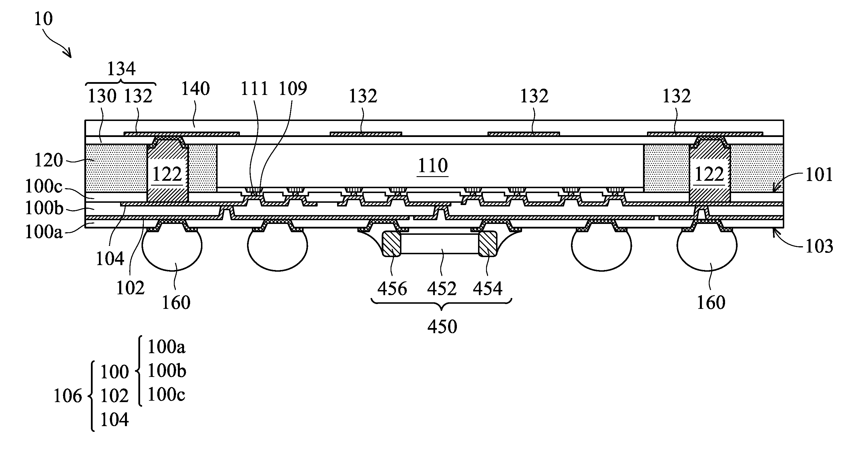
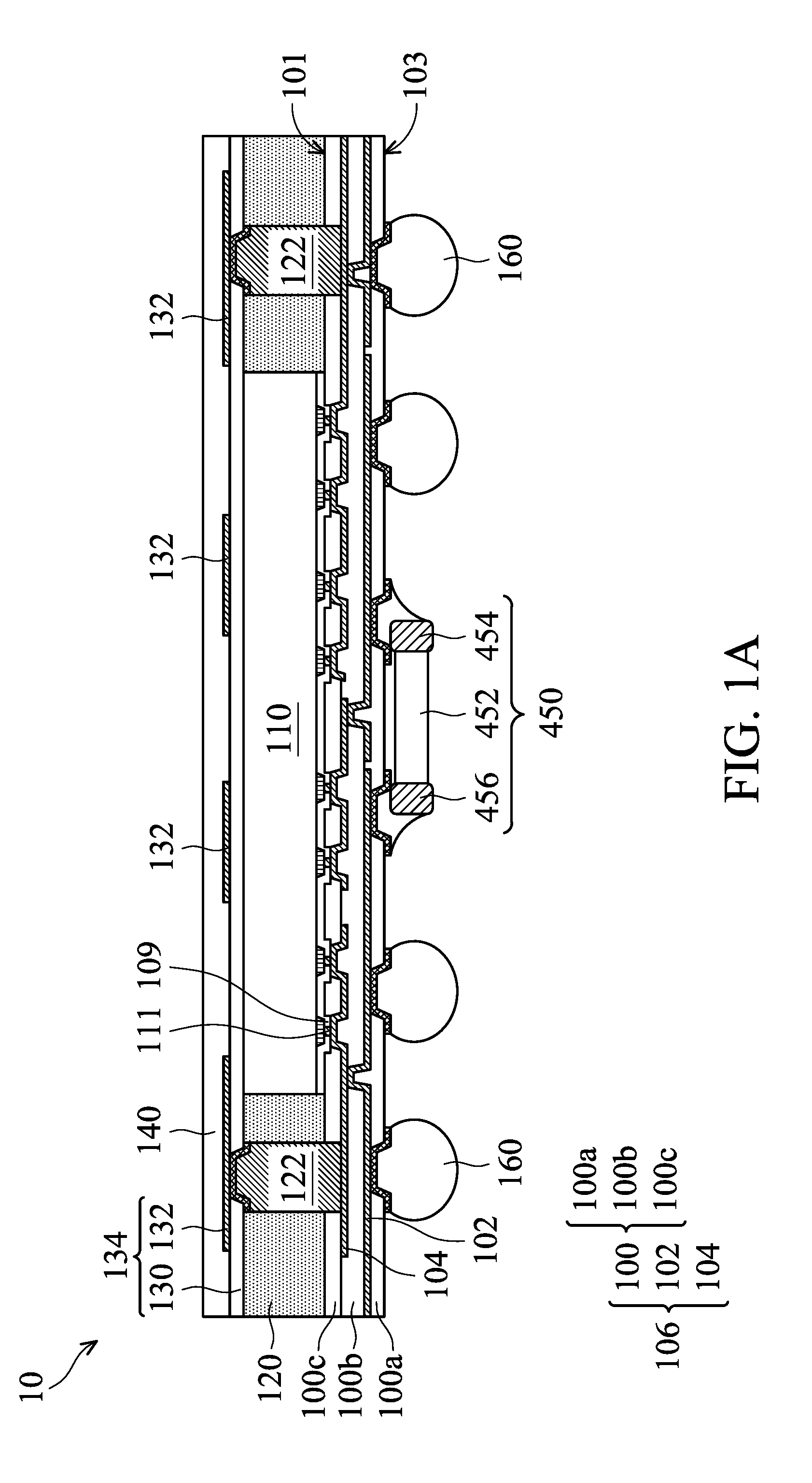
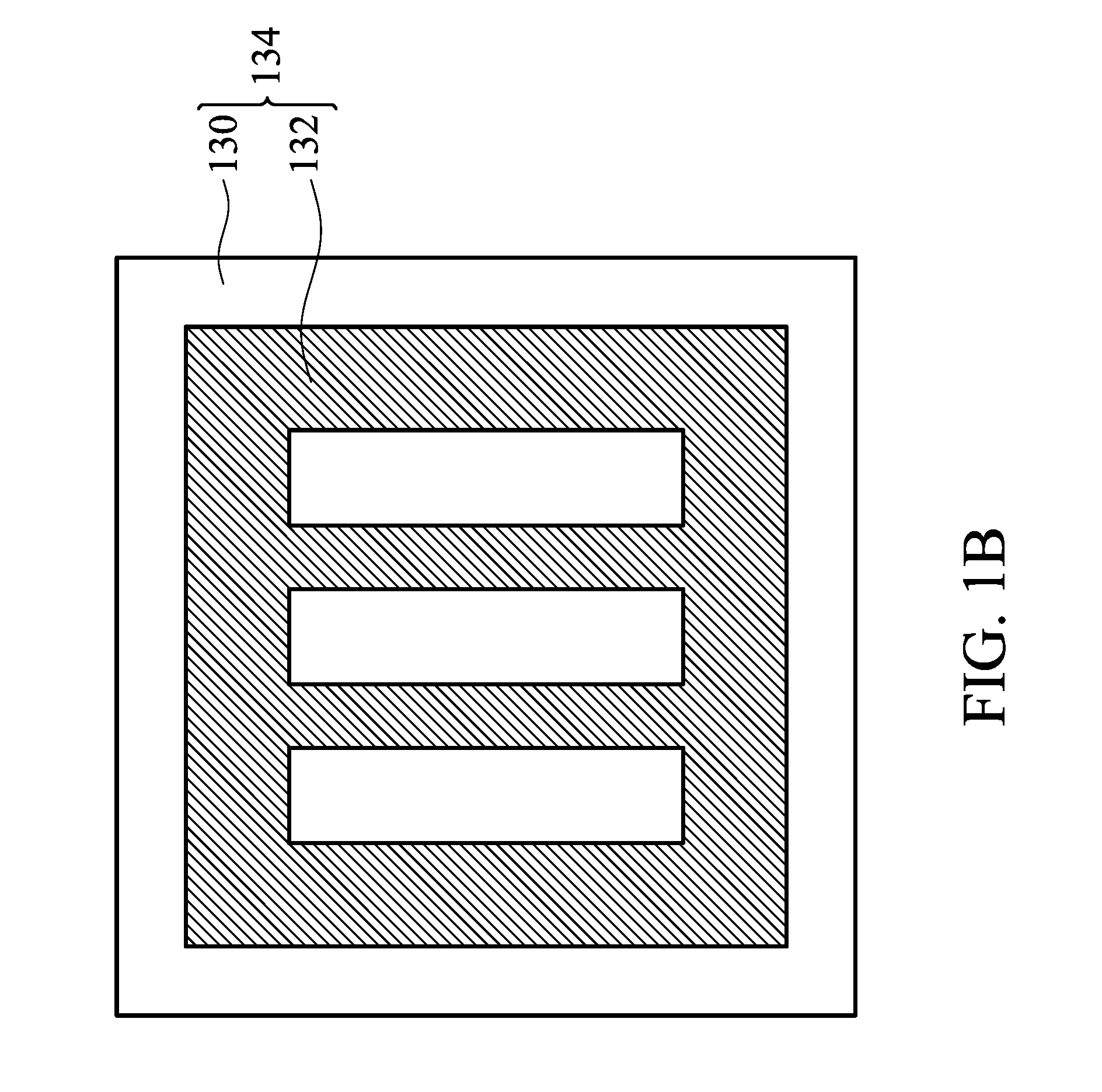
[0032]FIG. 1A is a cross-sectional view of a semiconductor package structure 10 in accordance with some embodiments of the disclosure. FIG. 1B is a plan view of an IMD structure 134 o...


PUM


Abstract

The invention provides a semiconductor package assembly. The semiconductor package assembly includes a first semiconductor package including a first redistribution layer (RDL) structure having a first surface and a second surface opposite to the first substrate. The first RDL structure includes a plurality of first conductive traces close to the first surface of the first RDL structure. An antenna pattern is disposed close to the second surface of the first RDL structure. A first semiconductor die is disposed on the first surface of the first RDL structure and electrically coupled to the first RDL structure. A plurality of conductive structures is disposed on the first surface of the first RDL structure and electrically coupled to the first RDL structure. The plurality of conductive structures is spaced apart from the antenna pattern through the plurality of first conductive traces of the first RDL structure.

Description

CROSS REFERENCE TO RELATED APPLICATIONS[0001]This application is a Continuation-In-Part of pending U.S. patent application Ser. No. 15 / 130,994, filed on Apr. 17, 2016, entitled “FAN-OUT PACKAGE STRUCTURE INCLUDING ANTENNA”, which claims the benefit of U.S. Provisional Application No. 62 / 157,046 filed on May 5, 2015 and U.S. Provisional Application No. 62 / 256,218 filed on Nov. 17, 2015. And this application also claims the benefit of U.S. Provisional Application No. 62 / 321,237 filed on Apr. 12, 2016 and U.S. Provisional Application No. 62 / 335,093 filed on May 12, 2016 the entirety of each of the above-identified priority applications are incorporated by reference herein.BACKGROUND OF THE INVENTION[0002]Field of the Invention[0003]The present invention relates to a semiconductor package assembly, and in particular to a fan-out semiconductor package with an antenna integrated into a single redistribution layer (RDL) structure.[0004]Description of the Related Art[0005]In order to ensure...

Claims


Application Information

Patent Timeline
Patent Type & Authority Applications(United States)
IPC IPC(8): H01L23/66H01L23/00H01L23/31H01L23/538
CPCH01L23/66H01L2225/1035H01L24/04H01L24/02H01L24/12H01L23/3114H01L2223/6677H01L2224/0401H01L2224/02379H01L2224/02381H01L2224/02373H01L2224/12105H01L25/0655H01L25/105H01L23/5389H01L23/5385H01L23/552H01L24/19H01L24/20H01L25/16H01L2224/04042H01L2224/04105H01L2224/32225H01L2224/73267H01L2924/1421H01L2924/1435H01L2924/1438H01L2924/19011H01L2924/19041H01L2924/19042H01L2924/19043H01L2924/3025H01L23/49816H01L23/5383H01L23/5384H01L2225/1041H01L2225/1058
Inventor LIN, TZU-HUNGPENG, I-HSUANLIU, NAI-WEIHUANG, WEI-CHECHOU, CHE-YA
Owner MEDIATEK INC
Why Eureka
Try Eureka