Light emitting device with epitaxial structure

a technology of light emitting device and epitaxial structure, which is applied in the direction of semiconductor devices, basic electric elements, electrical apparatus, etc., can solve the problems that the structural reliability of the product becomes less desirable, and achieve the effect of preferable structural reliability

Inactive Publication Date: 2017-03-09
PLAYNITRIDE
View PDF16 Cites 19 Cited by
  • Summary
  • Abstract
  • Description
  • Claims
  • Application Information

AI Technical Summary

Benefits of technology

[0006]The invention provides a light emitting device suitable to be disposed to various receiving substrates and having a preferable structural reliability.

Problems solved by technology

Thus, there may be dislocation between the epitaxial structure of the light emitting chip and the circuit board, and a structural reliability of the product consequently becomes less desirable.

Method used


Image

  • Light emitting device with epitaxial structure
  • Light emitting device with epitaxial structure
  • Light emitting device with epitaxial structure

Examples


Embodiment Construction

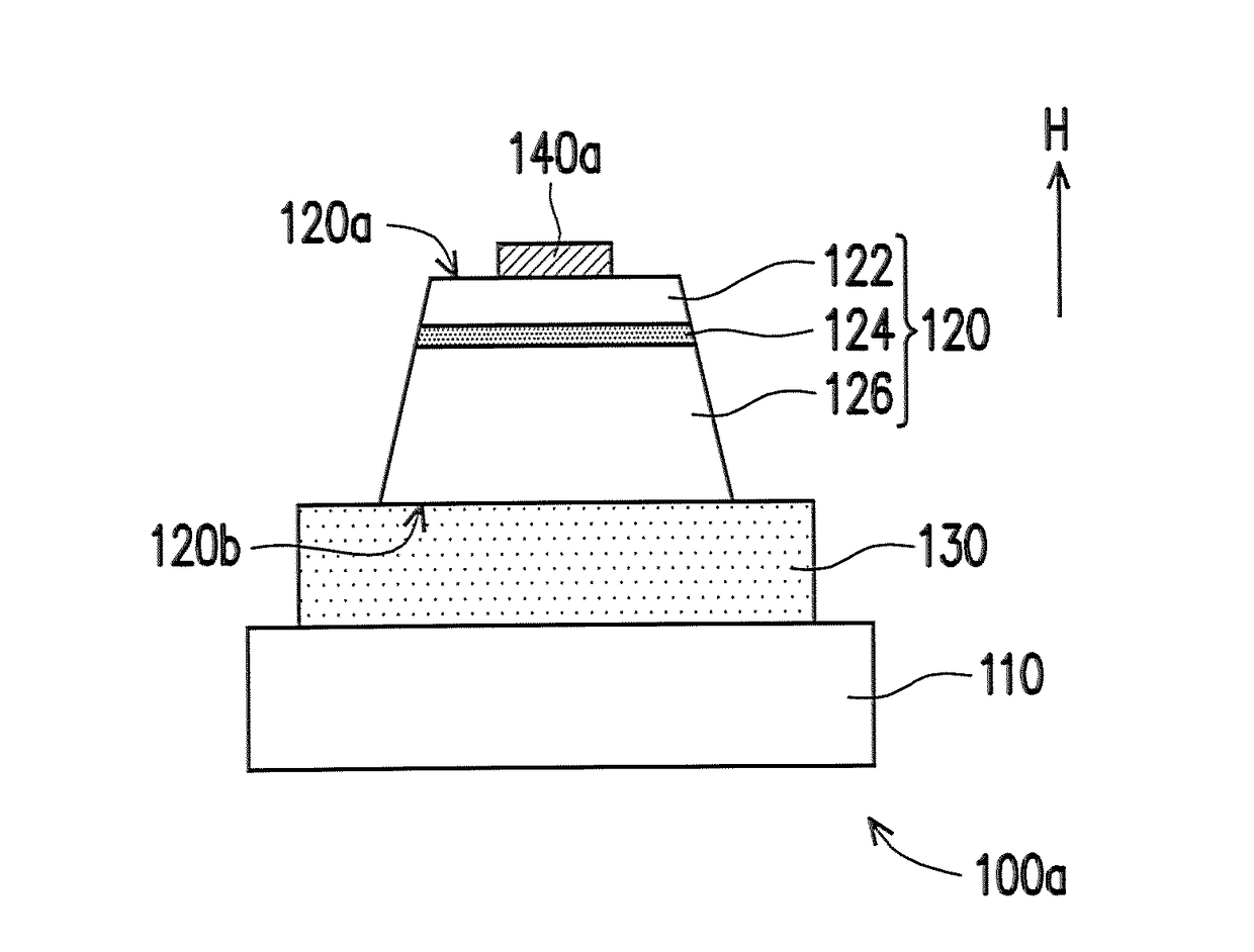
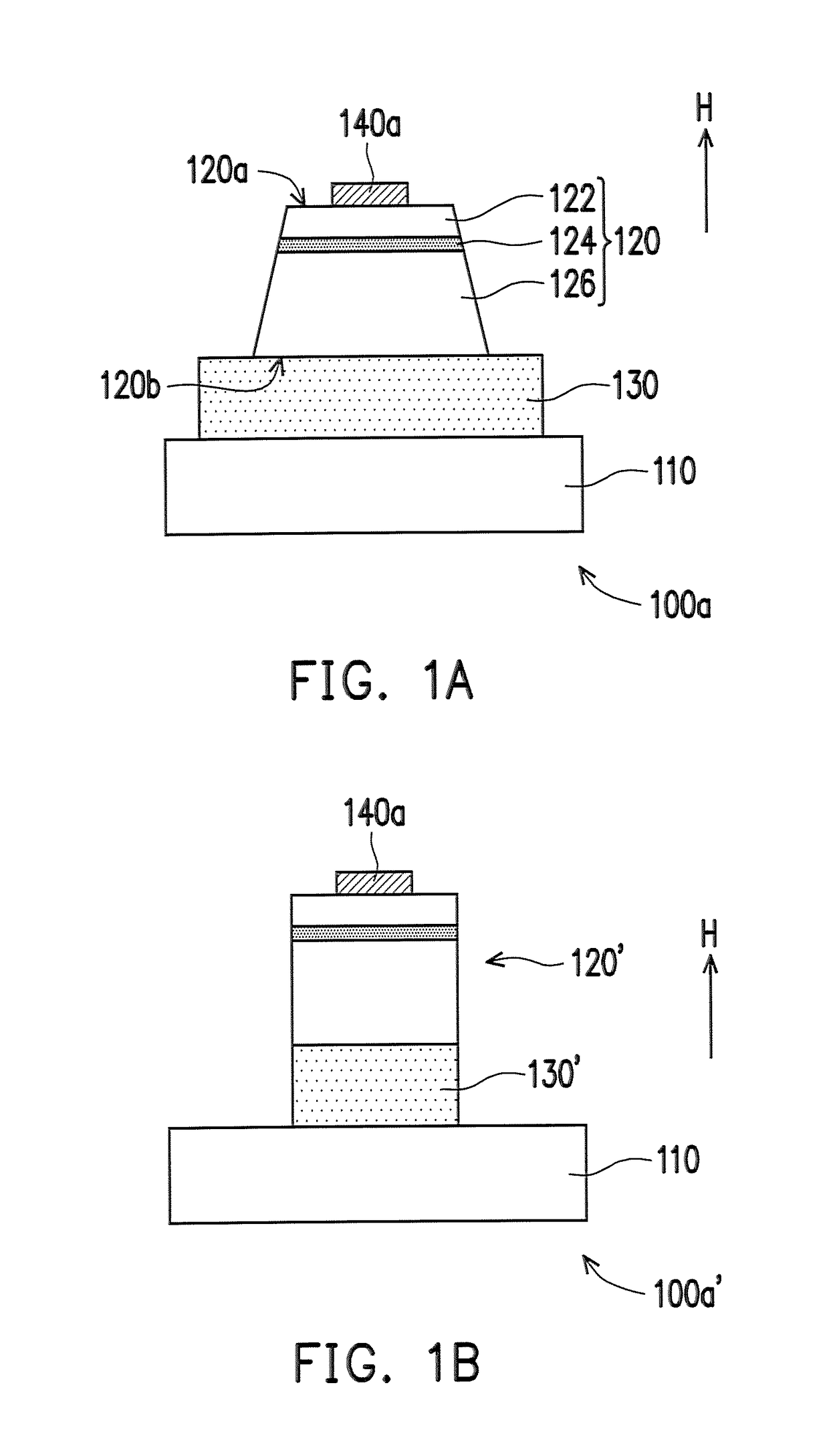
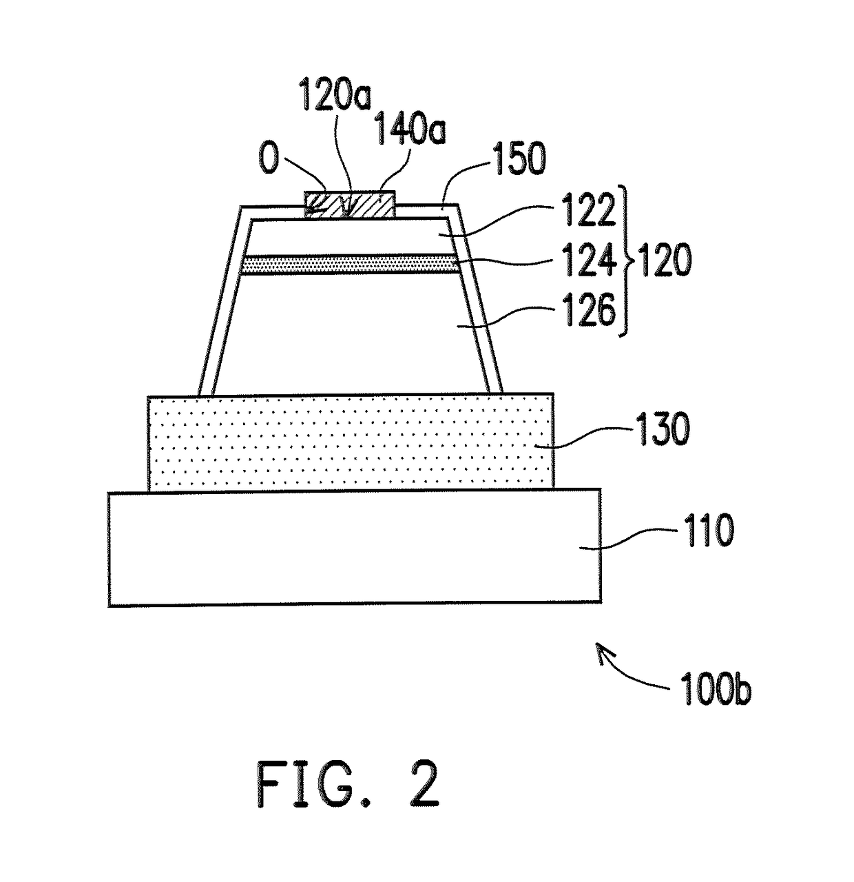
[0031]FIG. 1A is a schematic cross-sectional view illustrating a light emitting device according to an embodiment of the invention. Referring to FIG. 1A, in this embodiment, a light emitting device 100a includes a carrier 110, at least one epitaxial structure 120 (FIG. 1A only shows one epitaxial structure), at least one buffer pad 130 (FIG. 1A only shows one buffer pad 130), and at least one bonding pad 140a (FIG. 1A only shows one bonding pad 140a). The epitaxial structure 120 is disposed on the carrier 110. The buffer pad 130 is disposed between the carrier 110 and the epitaxial structure 120, wherein the epitaxial structure 120 is temporarily bonded to the carrier 110 by the buffer pad 130. The bonding pad 140a is disposed on the epitaxial structure 120, wherein the epitaxial structure 120 is electrically connected to a receiving substrate (not shown) through the bonding pad 140a.

[0032]Specifically, the carrier 110 of this embodiment is substantially a tentative substrate for t...


PUM


Abstract

A light emitting device includes a carrier, at least one epitaxial structure, at least one buffer pad and at least one bonding pad. The epitaxial structure is disposed on the carrier. The buffer pad is disposed between the carrier and the epitaxial structure, wherein the epitaxial structure is temporarily bonded to the carrier by the buffer pad. The bonding pad is disposed on the epitaxial structure, wherein the epitaxial structure is electrically connected to a receiving substrate by the bonding pad.

Description

CROSS-REFERENCE TO RELATED APPLICATION[0001]This application claims the priority benefit of Taiwan application serial no. 104129262, filed on Sep. 4, 2015. The entirety of the above-mentioned patent application is hereby incorporated by reference herein and made a part of this specification.BACKGROUND OF THE INVENTION[0002]Field of the Invention[0003]The invention relates to a semiconductor device, and particularly relates to a light emitting device.[0004]Description of Related Art[0005]In general, a light emitting chip is composed of an epitaxial structure, an N type electrode, and a P type electrode. In addition, the N type electrode and the P type electrode may respectively contact an N type semiconductor layer and a P type semiconductor layer. To make the light emitting chip more applicable, the light emitting chip that is manufactured may be heated for metal bonding to be fixed to a circuit board, so as to form a light emitting module. Due to a mismatch between thermal expansio...

Claims


Application Information

Patent Timeline
Patent Type & Authority Applications(United States)
IPC IPC(8): H01L33/40H01L27/15H01L33/38H01L33/62
CPCH01L33/40H01L33/387H01L27/156H01L33/62H01L25/0753H01L33/20H01L33/486H01L24/95H01L2224/0603H01L2224/95001H01L2224/80815H01L2224/80825H01L2224/08145H01L24/80H01L2224/08225H01L24/05H01L2924/12041H01L2924/14H01L2924/1304H01L24/08H01L2224/80006H01L33/0093H01L2224/05139H01L2224/0529H01L2224/05171H01L2224/05186H01L2224/05611H01L2224/05624H01L2224/05666H01L2224/05639H01L2224/05169H01L2224/05669H01L2224/058H01L2224/05144H01L2224/05638H01L2224/80409H01L2224/053H01L2224/05124H01L2224/05193H01L2224/0579H01L2224/05693H01L2224/05155H01L2224/05644H01L2224/05138H01L2224/05181H01L2224/80411H01L2224/05164H01L2224/05671H01L2224/05686H01L2224/05609H01L2224/05166H01L2224/05655H01L2224/05184H01L2224/95136H01L2924/00014H01L2924/013H01L2924/0542H01L2924/0103H01L2924/01074H01L2924/01022H01L2924/01015H01L2924/0549H01L2924/0544H01L2924/0105H01L2924/0543H01L2924/01049
Inventor LIN, TZU-YANGLAI, YU-HUNGLO, YU-YUN
Owner PLAYNITRIDE
Why Eureka
Try Eureka