Crystal growth method

Inactive Publication Date: 2003-09-23
SONY CORP
View PDF7 Cites 57 Cited by
  • Summary
  • Abstract
  • Description
  • Claims
  • Application Information

AI Technical Summary

Benefits of technology

In the first aspect of the invention, the mask layer can be formed as exposing part of the nitride semiconductor layer within the window region opened at part of the mask layer, and the exposed surface of the nitride semiconductor layer can be formed with irregularities within the window region. The irregularities act such that because of the discontinuity of the crystals formed at spaces established at the recessed portions of the irregularities, the through-type dislocations can be prevented from being propagated from the substrate side. The second nitride semiconductor layer is formed through crystal growth from the irregularities, and extends over a region including the upper surface of the mask layer. The growth over the region including the upper surface of the mask layer means crys

Problems solved by technology

However, the use of only these techniques using the low temperature buffer layer enables one to reduce the through-type dislocations, at most, to a level of about 10.sup.9 cm.sup.-2, thu

Method used


Image

  • Crystal growth method
  • Crystal growth method
  • Crystal growth method

Examples


Example

First Embodiment

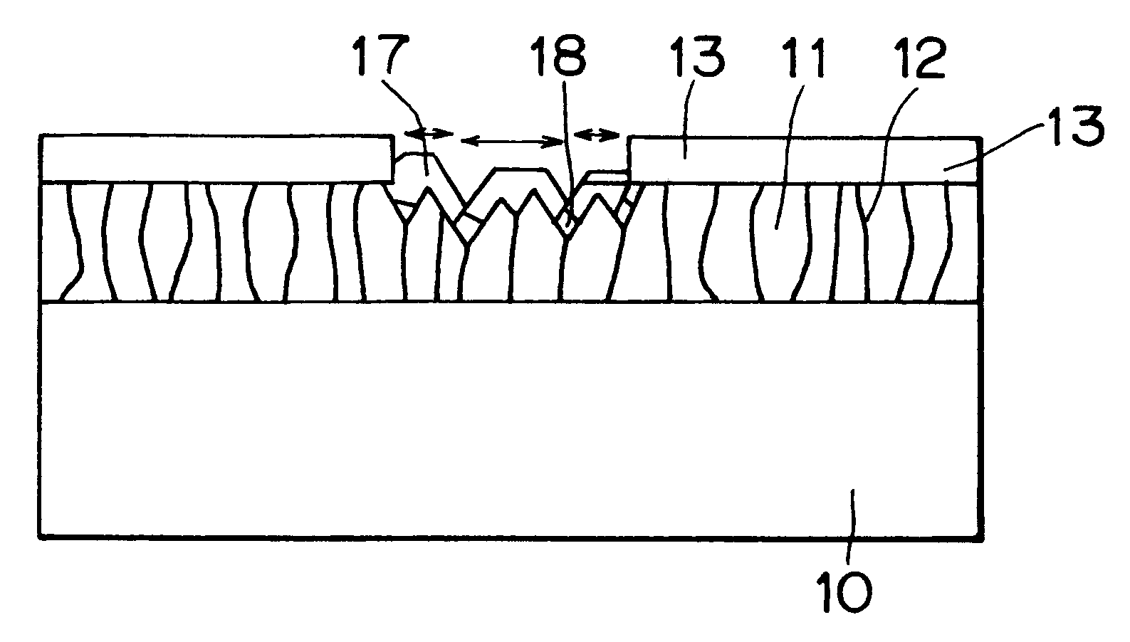
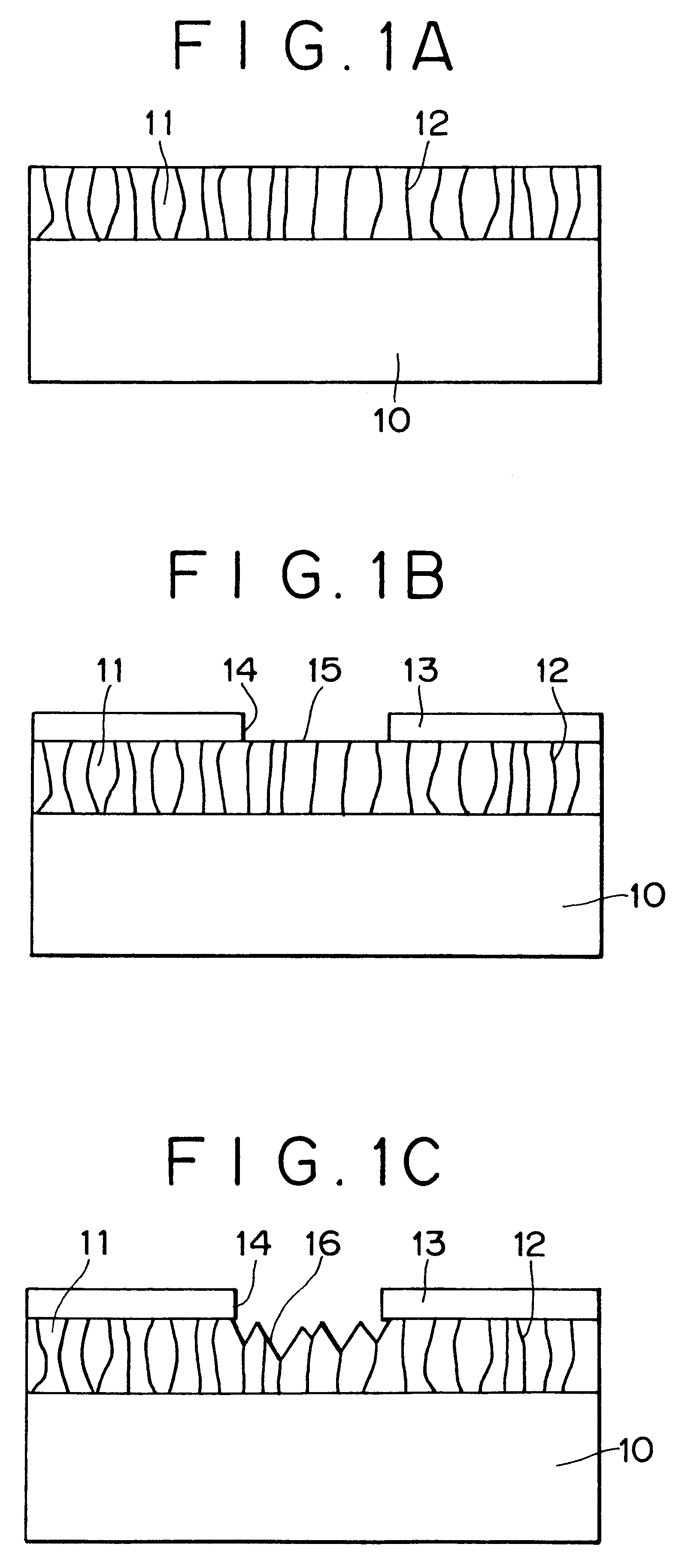
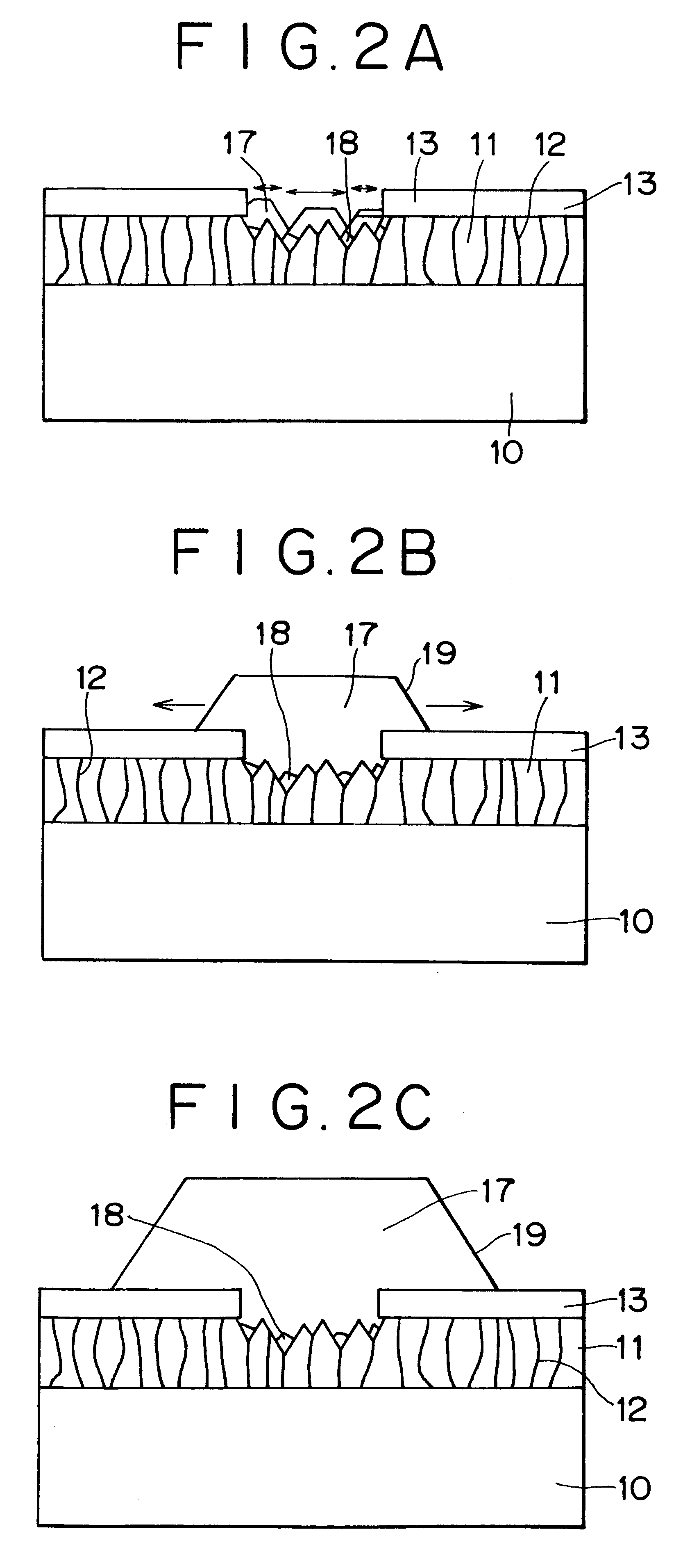
The first embodiment of the invention is now described with reference to FIGS. 1A to 1C and FIGS. 2A to 2C. Initially, as shown in FIG. 1A, an about 2 .mu.m thick epitaxial GaN layer 21 is grown as a first nitride semiconductor layer on a C face sapphire substrate 10 wherein the main surface of the substrate is a C+ face. Through-type dislocations 12 exist in the GaN layer 11 at a density of about 3.times.10.sup.9 cm.sup.-2 ascribed to the lattice-mismatching and the difference in coefficient of thermal expansion with the sapphire substrate 10.

Next, as shown in FIG. 1B, a mask layer 13 made of SiO.sub.2 is formed on the GaN layer 11. The mask layer 13 made of SiO.sub.2 has a thickness of about 20 nm. A window region 14 opened in the mask layer 13 according to a lithographic technique is formed. A surface 15 of the GaN layer 11 provided beneath the mask layer 13 is exposed to within the window region 14 formed by opening part of the mask layer 13 in a manner as set ou...

Example

Second Embodiment

The crystal growth method according to the second embodiment of the invention is described with reference to FIGS. 3A to 3C and FIGS. 4A to 4C. Like the first embodiment, as shown in FIG. 3A, an about 2 .mu.m thick epitaxial GaN layer 21 is grown as a first nitride semiconductor layer on a C face sapphire substrate 20 wherein the main surface of the substrate is a C+ face. Through-type dislocations 22 exist in the GaN layer 21 at a density of about 3.times.10.sup.9 cm.sup.-2 ascribed to the lattice-mismatching and the difference in coefficient of thermal expansion with the sapphire substrate 20.

Next, as shown in FIG. 3B, a mask layer 23 made of SiO.sub.2 is formed on the GaN layer 21. The mask layer 23 made of SiO.sub.2 has a thickness of about 20 nm. A window region 24 opened in the mask layer 23 according to a lithographic technique is formed. A surface 25 of the GaN layer 21 provided beneath the mask layer 23 is exposed to within the window region 24 formed by op...

Example

Third Embodiment

Next, the third embodiment of the invention is described with reference to FIGS. 5A and 5B, and FIGS. 6A to 6C. The crystal growth method of this embodiment is a modification of the crystal growth method of the second embodiment wherein when a first nitride semiconductor layer has been preliminarily grown on a sapphire substrate, a low temperature growth layer is finally formed to make an irregular surface, after which a mask layer is formed.

Like the first or second embodiment, as shown in FIG. 5A, an about 2 .mu.m thick epitaxial GaN layer 31 is grown as a first nitride semiconductor layer on a C face sapphire substrate 30 wherein the main surface of the substrate is a C+ face. Through-type dislocations 32 exist in the GaN layer 31 at a density of about 3.times.10.sup.9 cm.sup.-2 ascribed to the lattice-mismatching and the difference in coefficient of thermal expansion with the sapphire substrate 30.

Next, prior to formation of a mask layer, a low temperature growth ...


PUM


Abstract

A crystal growth method includes forming a mask layer capable of impeding crystal growth on a substrate in such a way a first nitride semiconductor layer has irregularities at a surface thereof exposed at a window region opened at a part of the mask layer, and growing a second nitride semiconductor layer over a region including the surface of the mask layer through crystal growth from the irregularities. Through-type dislocations can be reliably prevented from propagation due to the discontinuity of crystals at the irregularities and also to lateral crystal growth.

Description

The present application claims priority of Japanese Application No. P2000-217911 filed Jul. 18, 2000, which application is incorporated herein by reference to the extent permitted by law.BACKGROUND OF THE INVENTIONThis invention relates to a crystal growth method adapted for use in the formation of semiconductor light-emitting devices and more particularly, to a crystal growth method wherein selective crystal growth of a nitride semiconductor is carried out.Owing to the absence of either a lattice-matching substrate or a substrate of a low dislocation density in the vapor phase growth technology of a gallium nitride compound semiconductor, there is known a technique wherein after deposition of a buffer layer of AlN or Al.sub.x Ga.sub.1- N, in which 0.ltoreq.x<1, on a substrate such as of sapphire at a low temperature of 900.degree. C. or below, a gallium nitride compound semiconductor is grown to reduce the number of dislocations ascribed to the lattice-mismatching. Such a techni...

Claims


Application Information

Patent Timeline
IPC IPC(8): C30B25/02H01L21/20H01L21/02C30B29/38H01L21/205H01L33/22H01L33/32
CPCC30B25/02C30B29/403C30B29/406H01L21/0242H01L21/02458H01L21/02494H01L21/0254H01L21/0262H01L21/02639H01L21/02647
Inventor BIWA, GOSHIOKUYAMA, HIROYUKIDOI, MASATOOOHATA, TOYOHARU
Owner SONY CORP
Why Eureka
Try Eureka