Method of forming packaged lens modules

a technology of lens modules and packaging, applied in the field of semiconductor technology, can solve the problems of increasing the complexity of methods, physical damage to lenses, and degradation of imaging performance of camera modules being fabricated, and achieve the effects of improving efficiency, time saving, and process simplification

Active Publication Date: 2017-03-30
HOWE OPTOELECTRONICS TECH SHANGHAI
View PDF2 Cites 0 Cited by
  • Summary
  • Abstract
  • Description
  • Claims
  • Application Information

AI Technical Summary

Benefits of technology

The present invention provides a method for making packaged lens modules that is simpler, faster, and more efficient than conventional methods. The method provides for effective shielding during the filling of the gaps between the lens modules, eliminating the need for additional adhesive layers. Additionally, the use of a second mold plate that matches the size of sensor substrates to be attached to the lens modules allows for height adjustability and back focal length compensation of the packaged lens modules. The enclosure of the lens modules and the simplified process of injection molding result in simplified process and improved reliability of the product performance.

Problems solved by technology

These conventional methods of forming packaged lens modules include the steps of coating and removing the adhesive layer, thus increasing the complexity of the methods and may also bring risks of causing physical damages to the lens in the lens opening when removing the adhesive layer and / or causing imaging performance degradation of the camera modules being fabricated due to adhesive residues.

Method used


Image

  • Method of forming packaged lens modules
  • Method of forming packaged lens modules
  • Method of forming packaged lens modules

Examples


Embodiment Construction

[0030]The present invention will become apparent from the following detailed description of illustrative embodiments thereof, which is to be read in connection with the accompanying drawings. It is to be understood that the present invention is not limited to the embodiments set forth below and any alternative thereto generally known by those skilled in the art also falls in the scope of the invention.

[0031]In addition, the accompanying drawings that are merely intended to facilitate the explanation of the invention may not be drawn to scale for the sake of clarity or simplicity, and should thus not be construed as limiting the present invention in any way.

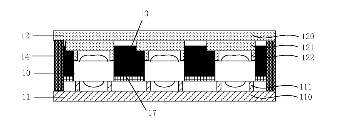
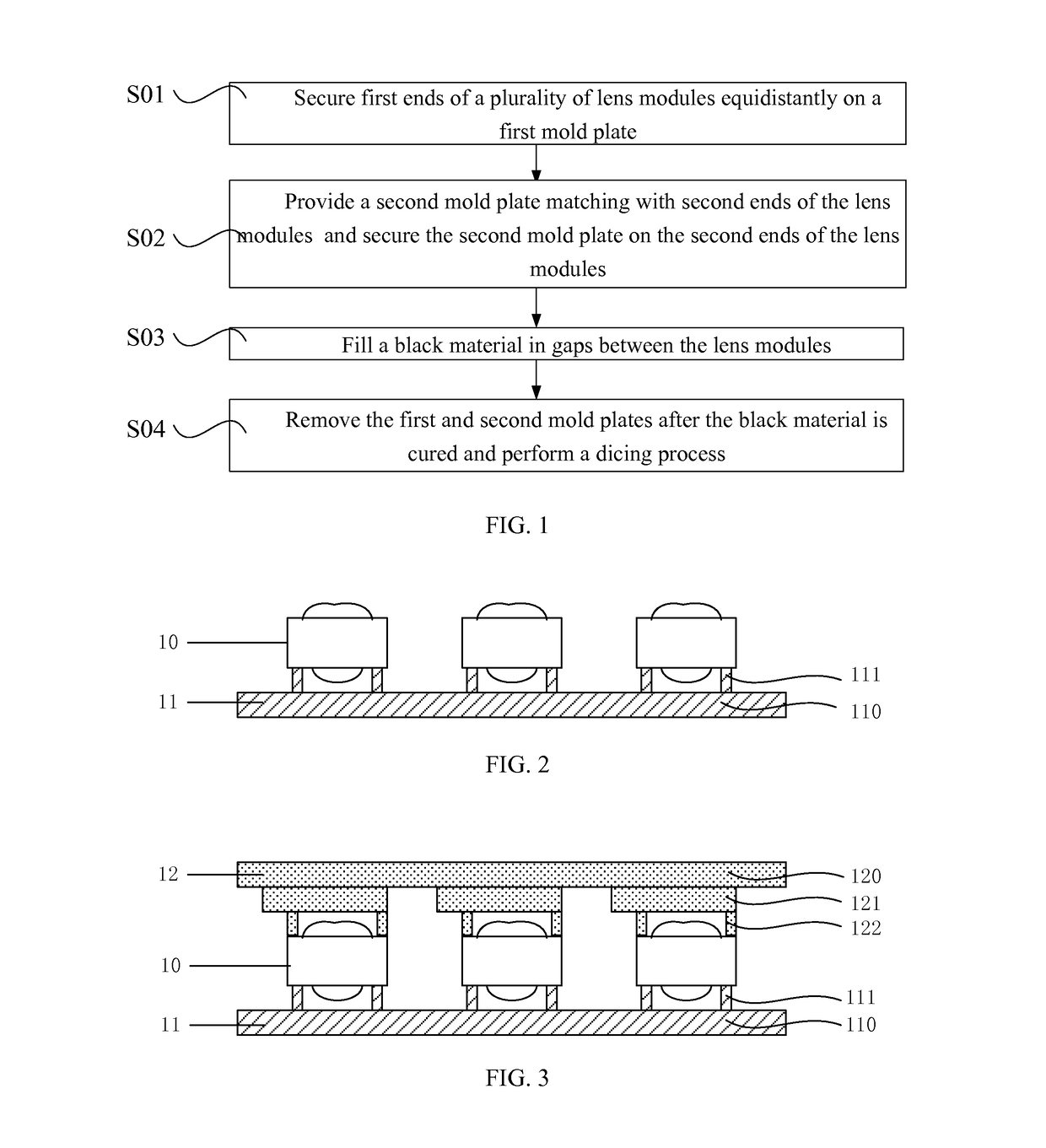
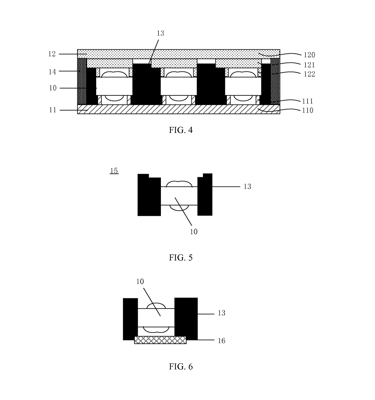
[0032]The core principle of the present invention is to simplify the conventional packaged lens module fabrication methods to make it more time-saving and more efficient by fixing a plurality of lens modules between a first mold plate and a second mold plate and filling a black material in gaps between the lens modules.

[0033]Refer...


PUM

PropertyMeasurementUnit
focal lengthsaaaaaaaaaa
back focal lengthaaaaaaaaaa

Abstract

A method of forming packaged lens modules is disclosed which includes: securing first ends of a plurality of lens modules equidistantly on a first mold plate; providing a second mold plate matching with second ends of the lens modules and securing the second mold plate on the second ends of the lens modules; filling a black material in gaps between the lens modules; and removing the first and second mold plates after the black material is cured and performing a dicing process. The method can effectively block lens openings to protect lenses from being contaminated and can eliminate the need for adhesive application and removal generally performed on second ends of the lens modules, thereby resulting in time savings and an efficiency improvement. Additionally, a height of the resulting packaged lens modules can be modified for back focal length compensation thereof by changing the size of the second mold plate.

Description

CROSS-REFERENCES TO RELATED APPLICATIONS[0001]This application claims the priority of Chinese patent application number 201410520715.X, filed on Sep. 30, 2014, the entire contents of which are incorporated herein by reference.TECHNICAL FIELD[0002]The present invention relates to the field of semiconductor technology, and more particularly to a method of forming packaged lens modules.BACKGROUND[0003]Digital cameras have been widely used in a variety of applications. With the advent of some new applications, such as cellular phones and medical appliances, digital cameras are miniaturized to be adapted for easy mounting. Accordingly, camera module, a component of digital cameras, is required to have low manufacturing cost and small horizontal and vertical occupation areas for its suitability for many applications. Such camera modules may be manufactured on a single wafer by using wafer-level technology and packaging technology, and then the wafer-level camera modules are singulated int...

Claims


Application Information

Patent Timeline
Patent Type & Authority Applications(United States)
IPC IPC(8): B29C45/16G02B7/20B29D11/00G02B13/00
CPCB29C45/1657B29D11/00009G02B7/20G02B13/001B29L2011/0016B29K2995/0025B29D11/00278B29D11/00807B29C39/10G02B13/0085B29C2793/0036B29C2793/009
Inventor FAN, REGIS
Owner HOWE OPTOELECTRONICS TECH SHANGHAI
Why Eureka
Try Eureka