Nanowire channel structures of continuously stacked heterogeneous nanowires for complementary metal oxide semiconductor (CMOS) devices

Inactive Publication Date: 2017-04-20
QUALCOMM INC
View PDF3 Cites 13 Cited by
  • Summary
  • Abstract
  • Description
  • Claims
  • Application Information

AI Technical Summary

Benefits of technology

[0016]In this regard, to provide a nanowire device with strong gate control but with a channel structure providing minimal fabrication and performance limitations, nanowire channel structures comprising continuously stacked heterogeneous nanowires for CMOS devices are provided. In particular, an exemplary nanowire CMOS device (“nanowire device”) includes a nanowire channel structure that includes a plurality of continuously stacked heterogeneous nanowires. Each of the plurality of continuously stacked heterogeneous nanowires is shaped to have a greater width at a central portion than at top and bottom end portions therein. Having continuously stacked nanowire structures eliminates the need to have a separation distance between vertically adjacent heterogeneous nanowires, thus providing a higher number of nanowires than a conventional nanowire device for a particular nanowire structure height. The greater number of heterogeneous nanowires provides increased gate control compared to the conventional nanowire device, but on a shorter nanowire channel structure, thus maintaining a lower parallel plate parasitic capacitance. Furthermore, the shorter nanowire channel structure simplifies fabrication compared to the conventional nanowire device.
[0017]Having the heterogeneous nanowires of the exemplary nanowire

Problems solved by technology

However, further scaling down of the conventional nanowire device is limited by a height of a nanowire channel structure therein.
In particular, scaling down of the nanowire device includes decreasing channel length, which results in increased leakage current and decreased gate control.
Accordingly, increasing the number of nanowires results in an increase in the height of the nanowire channel structure.
However, increasing the height of the nanowire channel structure may not be possible due to fabrication limitations associated with forming tall semiconductor structures and etching/forming nanowires therein.
Furthermore, even when possible, increasing the height of the

Method used


Image

  • Nanowire channel structures of continuously stacked heterogeneous nanowires for complementary metal oxide semiconductor (CMOS) devices
  • Nanowire channel structures of continuously stacked heterogeneous nanowires for complementary metal oxide semiconductor (CMOS) devices
  • Nanowire channel structures of continuously stacked heterogeneous nanowires for complementary metal oxide semiconductor (CMOS) devices

Examples


Example

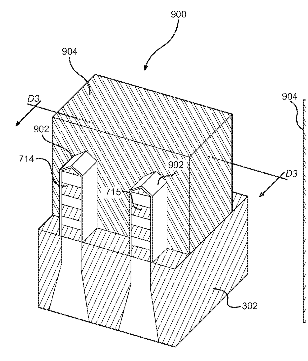
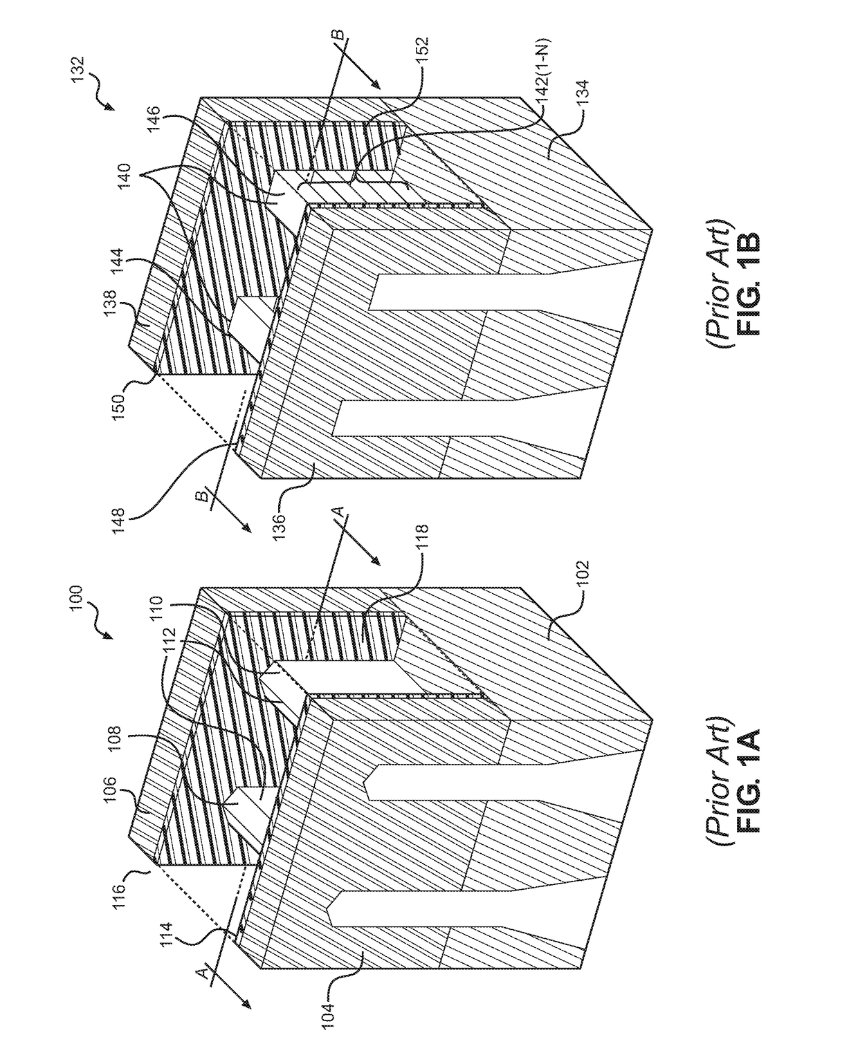
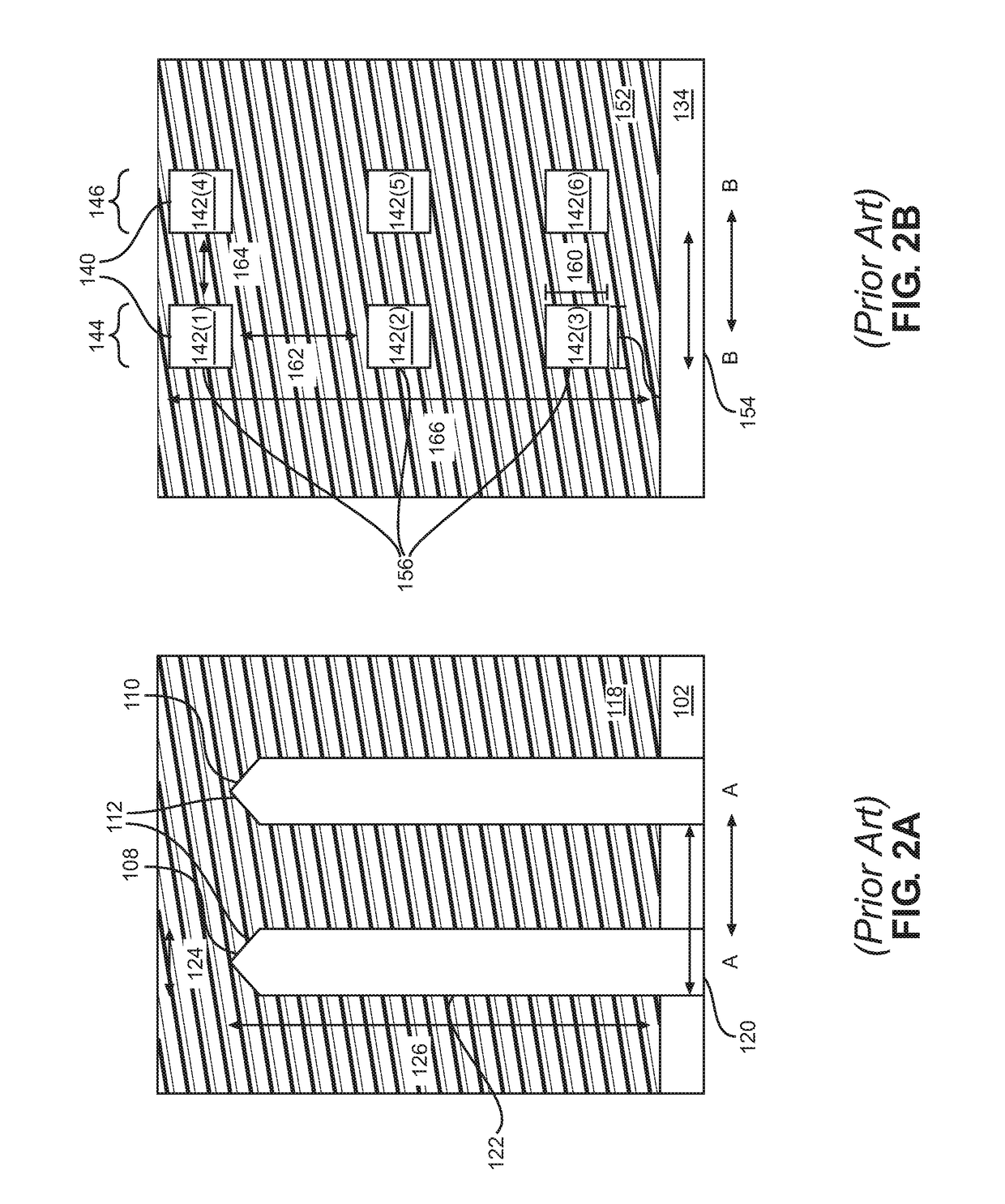
[0041]With reference now to the drawing figures, several exemplary aspects of the present disclosure are described. The word “exemplary” is used herein to mean “serving as an example, instance, or illustration.” Any aspect described herein as “exemplary” is not necessarily to be construed as preferred or advantageous over other aspects.

[0042]Aspects disclosed in the detailed description include nanowire channel structures of continuously stacked heterogeneous nanowires for complementary metal oxide semiconductor (CMOS) devices. A nanowire channel structure in a conventional nanowire device includes a plurality of nanowires, each nanowire completely surrounded by a gate material of a corresponding gate. This provides strong gate control and drive strength for a given footprint. However, further scaling down of the conventional nanowire device is limited by a height of a nanowire channel structure therein. In particular, scaling down of the nanowire device includes decreasing channel ...


PUM


Abstract

Aspects disclosed in the detailed description include nanowire channel structures of continuously stacked heterogeneous nanowires for complementary metal oxide semiconductor (CMOS) devices. Each of the nanowires has a top end portion and a bottom end portion that are narrower than a central portion. Furthermore, vertically adjacent nanowires are interconnected at the narrower top end portions and bottom end portions. This allows for connectivity between stacked nanowires and for having separation areas between vertically adjacent heterogeneous nanowires. Having the separation areas allows for gate material to be disposed over a large area of the heterogeneous nanowires and, therefore, provides strong gate control, a shorter nanowire channel structure, low parallel plate parasitic capacitance, and low parasitic channel capacitance. Having the nanowires be heterogeneous, i.e., fabricated using materials of different etching sensitivity, facilitates forming the particular cross section of the nanowires, thus eliminating the use of sacrificial masks/layers to form the heterogeneous nanowires.

Description

PRIORITY CLAIM[0001]The present application claims priority under 35 U.S.C. §119(e) to U.S. Provisional Patent Application Ser. No. 62 / 242,170 filed on Oct. 15, 2015 and entitled “CONTINUOUSLY STACKED NANOWIRE STRUCTURES FOR COMPLEMENTARY METAL OXIDE SEMICONDUCTOR (CMOS) DEVICES,” the contents of which is incorporated herein by reference in its entirety.RELATED APPLICATION[0002]The present application is related to U.S. patent application Ser. No. 15 / 198,763 filed on Jun. 30, 2016 and entitled “NANOWIRE CHANNEL STRUCTURES OF CONTINUOUSLY STACKED NANOWIRES FOR COMPLEMENTARY METAL OXIDE SEMICONDUCTOR (CMOS) DEVICES,” the contents of which is incorporated herein by reference in its entirety.BACKGROUND[0003]I. Field of the Disclosure[0004]This disclosure relates generally to complementary metal oxide semiconductor (CMOS) devices, and more specifically to implementing nanowire channel structures in CMOS devices.[0005]II. Background[0006]Transistors are essential components in modern elec...

Claims


Application Information

Patent Timeline
IPC IPC(8): H01L29/06H01L29/16H01L21/02H01L21/306H01L21/265H01L27/092H01L21/8238
CPCH01L29/0673H01L27/0924H01L29/0649H01L29/16H01L21/02603H01L21/30604H01L21/26506H01L21/823821H01L21/823807H01L29/66545H01L29/66795H01L29/7853H01L29/66439H01L29/125H01L29/045
Inventor XU, JEFFREY JUNHAOSONG, STANLEY SEUNGCHULYANG, DAMACHKAOUTSAN, VLADIMIRBADAROGLU, MUSTAFAYEAP, CHOH FEI
Owner QUALCOMM INC
Why Eureka
Try Eureka