Liquid Crystal Display Panel and Display

Active Publication Date: 2017-05-18
TCL CHINA STAR OPTOELECTRONICS TECH CO LTD +1
View PDF1 Cites 0 Cited by
  • Summary
  • Abstract
  • Description
  • Claims
  • Application Information

AI Technical Summary

Benefits of technology

[0016]The present invention adds the second pixel electrode and the second common electrode on the second substrate. The second pixel electrodes and the second common electrodes are staggered, and the horizontal electric fields are formed between the second pixel electrode

Problems solved by technology

However, for the horizontal electric field type liquid crystal display device, the electric field

Method used


Image

  • Liquid Crystal Display Panel and Display
  • Liquid Crystal Display Panel and Display
  • Liquid Crystal Display Panel and Display

Examples


embodiment 1

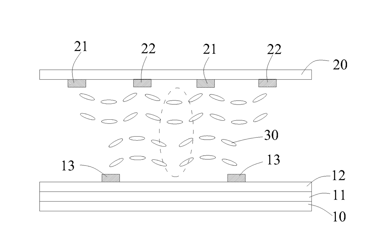
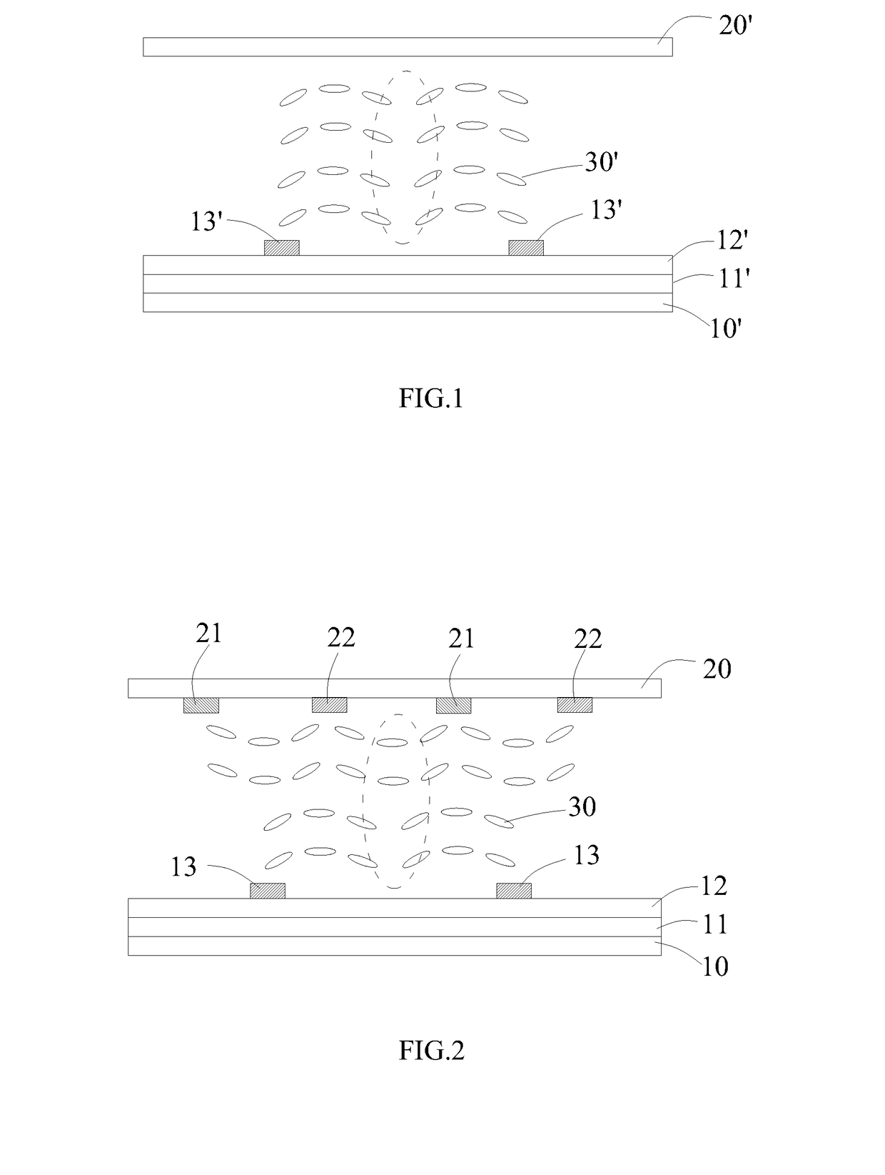
[0023]Referring to FIG. 2, in the Embodiment 1 of the present invention, the liquid crystal display panel comprises a first substrate 10 and a second substrate 20 opposed to each other, and a liquid crystal layer 30 located between the first substrate and the second substrate.

[0024]Wherein, the first substrate 10 is an array substrate, and the second substrate 20 is a color filter substrate. A first common electrode 11 and an insulating layer 12 are sequentially provided on the side of the first substrate 10 toward the second substrate 20. Multiple first pixel electrodes 13 are provided on the insulating layer 12, and the first pixel electrodes 13 are arrayed at equal intervals.

[0025]Furthermore, multiple second common electrodes 21 and multiple second pixel electrodes 22 are provided on the side of the second substrate 20 toward the first substrate 10, and the second common electrodes 21 and the second pixel electrodes 22 are provided at intervals.

[0026]Specifically, in the present...

embodiment 2

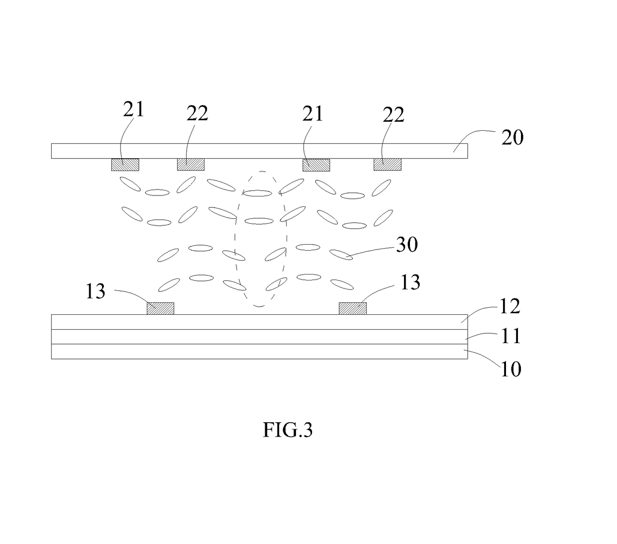
[0028]Referring to FIG. 3, in the Embodiment 2 of the present invention, the liquid crystal display panel also comprises a first substrate 10 and a second substrate 20 opposed to each other, and a liquid crystal layer 30 located between the first substrate and the second substrate.

[0029]Wherein, the first substrate 10 is an array substrate, and the second substrate 20 is a color filter substrate. A first common electrode 11 and an insulating layer 12 are sequentially provided on the side of the first substrate 10 toward the second substrate 20. Multiple first pixel electrodes 13 are provided on the insulating layer 12, and the first pixel electrodes 13 are arrayed at equal intervals.

[0030]Multiple second common electrodes 21 and multiple second pixel electrodes 22 are provided on the side of the second substrate 20 toward the first substrate 10, and the second common electrodes 21 and the second pixel electrodes 22 are provided at intervals.

[0031]In the present embodiment, the secon...


PUM


Abstract

The present invention discloses a liquid crystal display panel and a display. The display panel comprises a first substrate and a second substrate opposed to each other, and a liquid crystal layer located between the first substrate and the second substrate. A first common electrode and an insulating layer are sequentially provided on the side of the first substrate toward the second substrate. Multiple first pixel electrodes are provided on the insulating layer. Multiple second common electrodes and multiple second pixel electrodes are provided on the side of the second substrate toward the first substrate. The second common electrodes and the second pixel electrodes are provided at intervals. In present invention, the tilted liquid crystal molecules at obscure position tends to be horizontally aligned, which increases the light transmittance at the obscure position and eliminates the obscure in the liquid crystal display panel and display.

Description

BACKGROUND OF THE INVENTION[0001]1. Field of the Invention[0002]The present invention relates to the field of liquid crystal displaying techniques, and in particular to a liquid crystal display panel.[0003]2. The Related Arts[0004]According to the direction of the electric field driving the liquid crystal, the liquid crystal display device is divided into a vertical electric field type liquid crystal display device and a horizontal electric field type liquid crystal display device. Vertical electric field type liquid crystal display device includes a twisted nematic (TN) mode and a vertical alignment (VA) mode. The horizontal electric field type liquid crystal display device includes an in-plane switching (IPS) mode, the fringe field switching (FFS) mode and advanced super-dimensional field switching (ADS) mode. With respect to the vertical electric field type liquid crystal display device, horizontal electric field type liquid crystal display device does not require additional opti...

Claims


Application Information

Patent Timeline
IPC IPC(8): G02F1/1343G02F1/1335G02F1/1333
CPCG02F1/134363G02F1/133345G02F2201/121G02F2201/123G02F1/133514G02F1/134372
Inventor XIE, CHANG
Owner TCL CHINA STAR OPTOELECTRONICS TECH CO LTD
Why Eureka
Try Eureka