

Electronic device and method of manufacturing electronic device, and electronic apparatus
a technology of electronic devices and manufacturing methods, applied in the direction of electroluminescent light sources, organic semiconductor devices, electric lighting sources, etc., can solve the problem of difficulty in achieving the intended insulating property of wiring patterns
- Summary
- Abstract
- Description
- Claims
- Application Information
AI Technical Summary
Benefits of technology
Problems solved by technology
Method used
Image

Examples
embodiment
1. EMBODIMENT
(1-1. Overall Configuration)
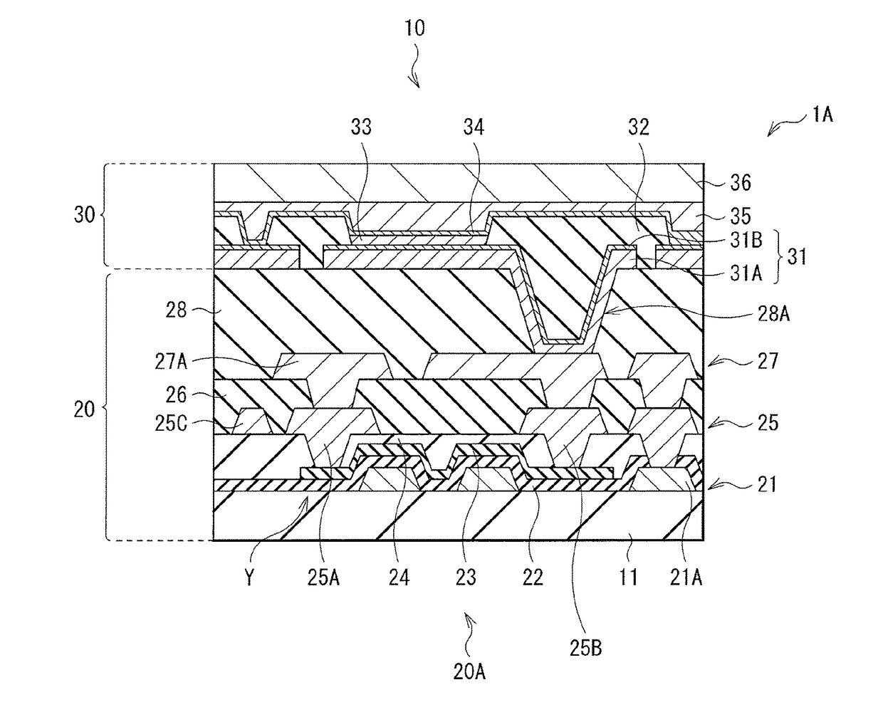
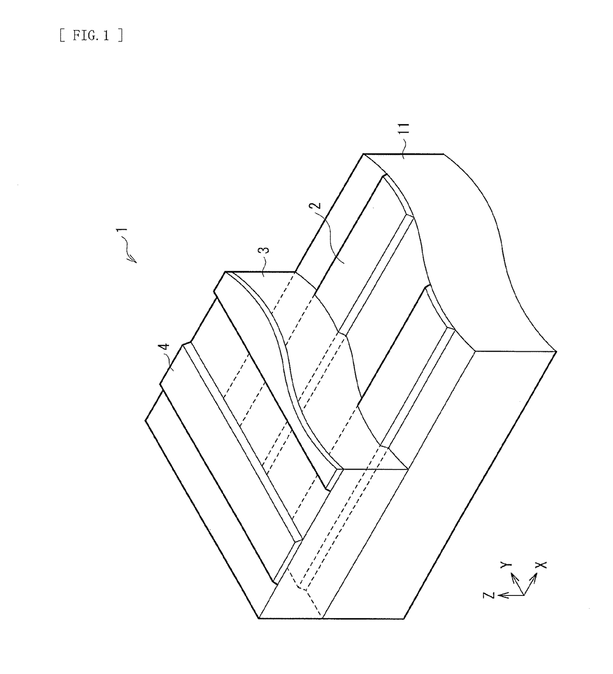
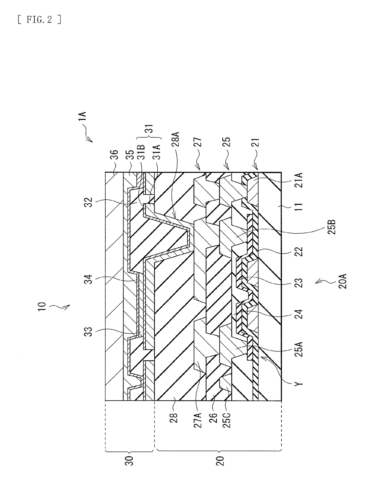
[0029]FIG. 1 illustrates a perspective view of a cross-sectional configuration of an electronic device (an electronic device 1) according to an embodiment of the disclosure. In the electronic device, a lower-layer wiring pattern 2 (a first wiring pattern) and an upper-layer wiring pattern 4 (a second wiring pattern) are laminated with an organic insulating layer 3 interposed between. The plurality of lower-layer wiring patterns 2 are provided on a substrate 11. The lower-layer wiring patterns 2 are disposed in such a manner that the lower-layer wiring patterns 2 are electrically coupled to each other partially, and each extend in one direction, for example, X-axis direction (a first direction). FIG. 2 illustrates a cross-sectional configuration of a display unit (a display unit 1A) that includes a display device that is an example of the electronic device 1 illustrated in FIG. 1. The display unit 1A may be used as, for example, an organic EL ...
application examples
2. APPLICATION EXAMPLES
[0070]The electronic device 1 (for example, the display unit 1A provided with a display device) that is described in the above-described embodiment may be preferably usable optimally as the following electronic apparatuses, for example.
application example 1
[0071]FIG. 10A illustrates an external appearance a tablet to which the display unit 1A according to the above-described embodiment is applied viewed from front side thereof, and FIG. 10B illustrates the external appearance of the tablet viewed from rear side thereof. This tablet may include, for example, a display section 610 (the display unit 1A) and a non-display section (a chassis) 620, as well as an operation section 630. The operation section 630 may be provided on the front surface of the non-display section 620 as illustrated in FIG. 10A, or may be provided on the top surface as illustrated in FIG. 10B.
PUM
 Abstract
Description
Claims
Application Information