System and method in indium-gallium-arsenide channel height control for sub 7nm finfet

a technology of indium gallium arsenide and channel height control, which is applied in the direction of semiconductor devices, electrical equipment, basic electric elements, etc., can solve the problems of poor control, unsuitable high temperature thermal removal process, and unsuitable wet etching

Inactive Publication Date: 2017-08-03
APPLIED MATERIALS INC
View PDF0 Cites 0 Cited by
  • Summary
  • Abstract
  • Description
  • Claims
  • Application Information

AI Technical Summary

Benefits of technology

[0008]In one embodiment, a method includes exposing an oxide layer formed on a substrate to a first plasma, exposing the oxide layer to a second plasma to convert the oxide layer to an evaporable layer at a first temperature, evaporating the evaporable layer at a second temperature higher than the first temperature to expose a surface of a group III-V semiconductor material, and exposing the surface of the group III-V semiconductor material to an oxygen containing gas.
[0009]In another embodiment, a method includes breaking oxygen bonds in an oxide layer, converting the oxide layer to an evaporable layer at a first temperature, evaporating the evaporable layer at a second temperature higher than the first temperature to expose a surface of a group III-V semiconductor material, and oxidizing the surface of the group III-V semiconductor material.
[0010]In another embodiment, a method includes a) exposing an oxide layer to a first plasma, b) exposing the oxide layer to a second plasma to convert the oxide layer to an evaporable layer at a first temperature, c) evaporating the evaporable layer at a second temperature higher than the first temperature to expose a surface of a group III-V semiconductor material, d) exposing the surface of the group III-V semiconductor material to an oxygen containing gas, e) iteratively repeating at least a-c, and f) forming a channel material on the substrate.

Problems solved by technology

High temperature thermal removal process is not suitable because of As diffusion and In / Ga segregation at high temperatures, as well as pits formation on the surface.
Wet etch is not suitable because wet etch is typically performed ex-situ and is not good to control group III-V semiconductors recess depth with different feature sizes.
High power RF plasma etch can damage the surface and causing residual oxygen implanting, as well as large etch depth loading.

Method used


Image

  • System and method in indium-gallium-arsenide channel height control for sub 7nm finfet
  • System and method in indium-gallium-arsenide channel height control for sub 7nm finfet
  • System and method in indium-gallium-arsenide channel height control for sub 7nm finfet

Examples


Embodiment Construction

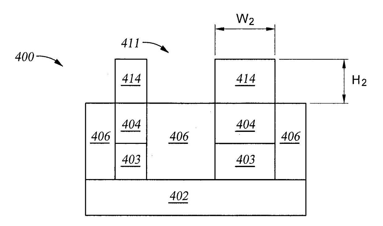
[0017]A method for forming a group III-V semiconductor channel region in a transistor is provided herein. The method includes exposing an oxide layer present on a substrate to a first plasma to treat the oxide layer, exposing the treated oxide layer to a second plasma to convert the oxide layer to an evaporable layer, evaporating the evaporable layer to expose a group III-V semiconductor material surface, and exposing the group III-V semiconductor material surface to an oxygen containing gas to oxidize the group III-V semiconductor material. The processes may be repeated until a recessed depth having a predetermined depth is formed. A group III-V semiconductor channel is then formed in the predetermined recessed depth. The control of the height of the group III-V semiconductor channel is improved. Additionally, the method also provides excellent selectivity and profile control.

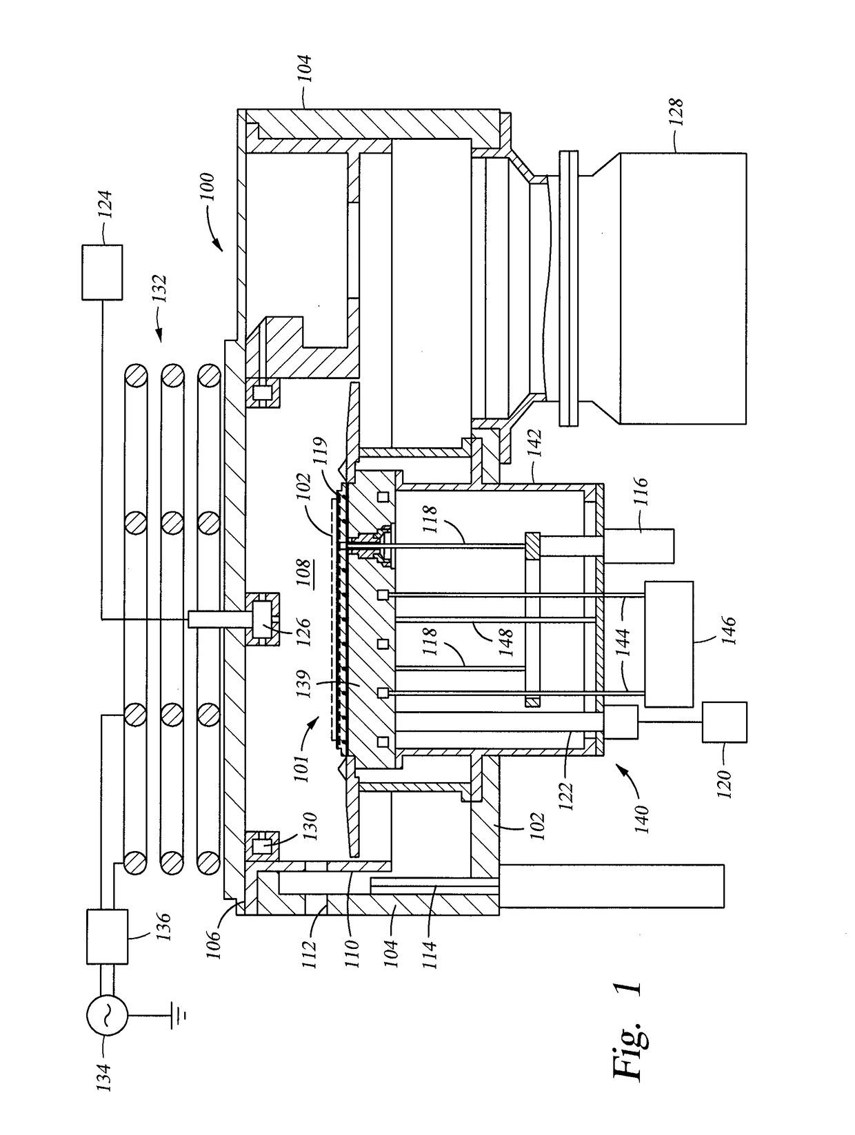
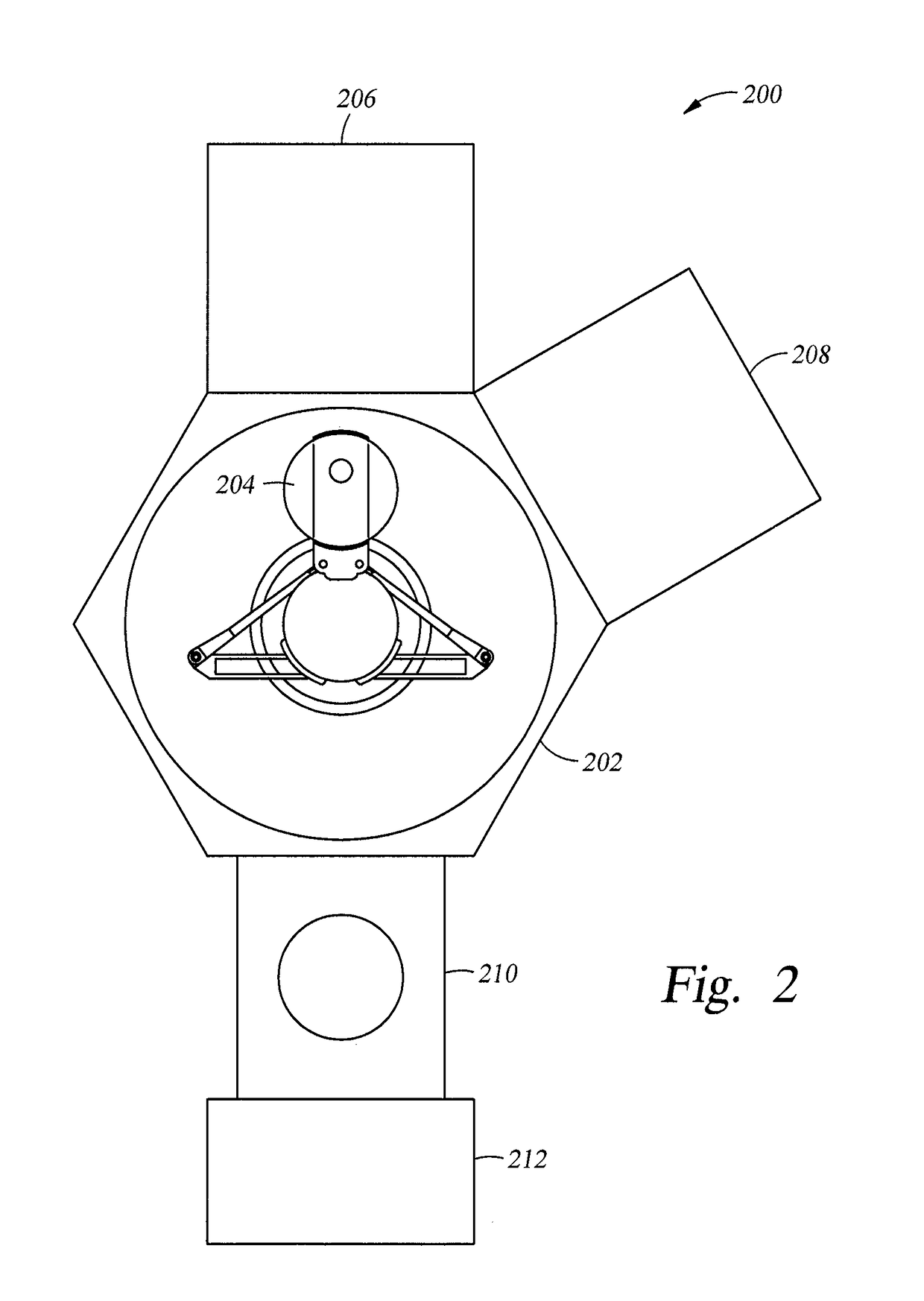
[0018]FIG. 1 is a schematic, cross-sectional view of a plasma processing chamber 100 within which the metho...


PUM

PropertyMeasurementUnit
temperatureaaaaaaaaaa

Abstract

A method for forming a group III-V semiconductor channel region in a transistor is provided herein. The method includes exposing a substrate including an oxide layer to a first plasma to treat the oxide layer, exposing the treated oxide layer to a second plasma to convert the oxide layer to an evaporable layer, evaporating the evaporable layer to expose a group III-V semiconductor material surface, and exposing the group III-V semiconductor material surface to an oxygen containing gas to oxidize the group III-V semiconductor material. The processes may be repeated until a recessed depth having a predetermined depth is formed. A group III-V semiconductor channel is then formed in the predetermined recessed depth. The control of the height of the group III-V semiconductor channel is improved.

Description

CROSS-REFERENCE TO RELATED APPLICATIONS[0001]This application claims priority to U.S. Provisional Patent Application Ser. No. 62 / 288,120, filed on Jan. 28, 2016, which herein is incorporated by reference.BACKGROUND[0002]Field[0003]Embodiments of the present disclosure generally relate to methods and apparatus for forming a semiconductor device. More specifically, embodiments described herein relate to a method for controlling channel height in a transistor.[0004]Description of the Related Art[0005]As circuit densities increase for next generation devices, the widths of interconnects, such as vias, trenches, contacts, gate structures and other features, as well as the dielectric materials therebetween, decrease to 7 nm or smaller dimensions, whereas the thickness of the dielectric layers remain substantially constant, with the result of increasing the aspect ratios of the features. Recently, complementary metal oxide semiconductor (CMOS) devices having fin field-effect transistors (F...

Claims


Application Information

Patent Timeline
Patent Type & Authority Applications(United States)
IPC IPC(8): H01L21/02H01L21/3105H01L29/66
CPCH01L21/02546H01L29/66795H01L21/02664H01L21/3105H01L21/0234H01L21/02241H01L21/02252H01L21/02255H01L21/30621H01L21/31122
Inventor YAN, CHUNBAO, XINYU
Owner APPLIED MATERIALS INC
Why Eureka
Try Eureka