Power semiconductor module having a pressure application body and arrangement therewith

a technology of power semiconductor modules and application bodies, which is applied in the direction of semiconductor devices, semiconductor device details, electrical apparatus, etc., can solve the problems of limited current carrying capacity of known pressure contact springs, and achieve the effect of increasing the current carrying capacity of connecting elements, reducing the loss of flexibility or compactness

Active Publication Date: 2017-08-03
SEMIKRON ELECTRONICS GMBH & CO KG
View PDF4 Cites 2 Cited by
  • Summary
  • Abstract
  • Description
  • Claims
  • Application Information

AI Technical Summary

Benefits of technology

[0005]It is an object of the invention is to provide an improved power semiconductor module which has an essentially higher current carrying capacity of the connecting elements than heretofore known, without loss of flexibility or compactness.

Problems solved by technology

A deficiency with such configurations is the limited current carrying capacity of the known pressure contact springs 68, which capacity is correspondingly approximately 10 A in the prior art.

Method used


Image

  • Power semiconductor module having a pressure application body and arrangement therewith
  • Power semiconductor module having a pressure application body and arrangement therewith
  • Power semiconductor module having a pressure application body and arrangement therewith

Examples


Embodiment Construction

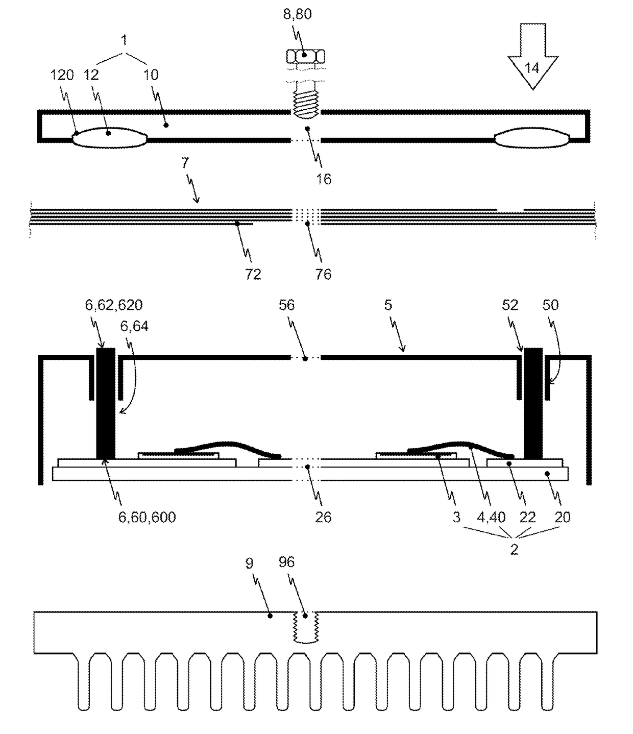
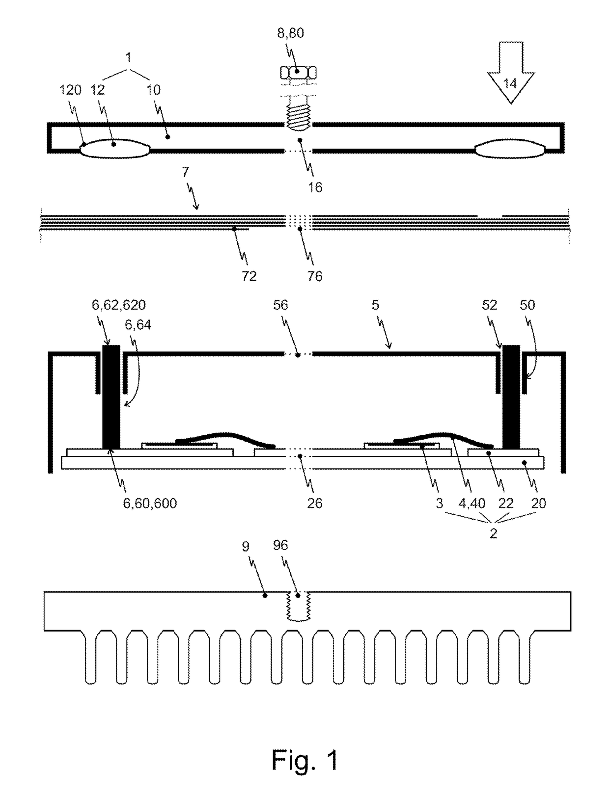
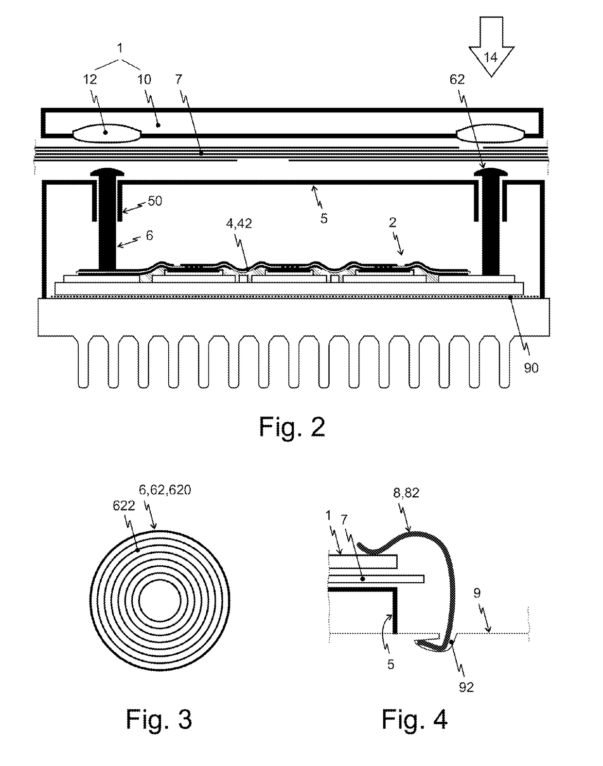
[0030]FIG. 1 shows a first refinement of a power semiconductor module according to the invention in a first arrangement according to the invention in an exploded illustration. The arrangement has here the following components: a clamping device 8, a pressure application body 1 of the power semiconductor module, a circuit board 7, a housing 5 of the power semiconductor module with circuit carrier 2 arranged therein, and a cooling device 9. Circuit board 7 is arranged here between housing 5 and pressure application body 1.

[0031]Cooling device 9 is embodied as an air cooling device with a cutout 96 which has an internal thread. Housing 5 of the power semiconductor module is embodied here in a beaker-like fashion and covers circuit carrier 2 towards cooling device 9. Housing 5 has two guide devices 50 in each of which an assigned connecting element 6 is arranged here.

[0032]Circuit carrier 2 is embodied with a substrate 20 which has conductor tracks 22 with separated potential from one a...


PUM


Abstract

A power semiconductor module having a pressure application body, a circuit carrier, which is embodied with a first conductor track, a power semiconductor element arranged thereon and an internal connecting device, and also having a housing which is embodied with a guide device arranged therein, with a connecting element. The connecting element is embodied as a bolt with first and second end sections and an intermediate section therebetween, wherein the first end section rests on the circuit carrier and is electrically conductively connected thereto; the second end section projects out of the housing through a cutout; and wherein the connecting element is arranged in the assigned guide device. The pressure application body has a first rigid partial body and a second elastic partial body, wherein the second partial body protrudes out of the first partial body in the direction of the housing.

Description

BACKGROUND OF THE INVENTION[0001]1. Field of the Invention[0002]The invention is directed to a power semiconductor module having a pressure application body, having a circuit carrier which is embodied with a first conductor track, a power semiconductor component arranged thereon, and having an internal connecting device. The power semiconductor module also has a housing having a guide device arranged therein, in particular for a connecting element which serves to connect the circuit carrier to an external connecting device, in particular an external circuit board with load current conductor tracks. In addition, the power semiconductor module has a pressure application body for applying pressure to the circuit carrier. In an arrangement with this power semiconductor module, the pressure body serves for bringing about thermal and mechanical connection of the circuit carrier to a cooling device.[0003]2. Description of the Related Art[0004]The prior art, disclosed, for example, in Germa...

Claims


Application Information

Patent Timeline
Patent Type & Authority Applications(United States)
IPC IPC(8): H01L23/10H01L23/40H01L23/00H01L23/049H01L23/495H01L25/065
CPCH01L23/10H01L23/49531H01L25/0655H01L23/49575H01L23/4951H01L24/48H01L2023/405H01L23/49568H01L23/049H01L23/4006H01L2224/48245H01L2023/4025H01L2023/4087H01L23/49517H01L23/04H01L23/34H01L23/48H01L23/053H01L2224/48472H05K7/209H01L2924/00014H01L23/3735H01L23/49811H01L24/01H01L24/73H01L2224/48227H01L2224/73265H01L25/072H01L25/18H01L2224/05599H01L2224/45099H01L2224/85399H01L2224/32225H01L2924/00012
Inventor GOBL, CHRISTIANVENNEBUSCH, CLEMENS
Owner SEMIKRON ELECTRONICS GMBH & CO KG
Why Eureka
Try Eureka