Display device and driving method thereof

a technology of a display device and a driving method, which is applied in the direction of instruments, static indicating devices, etc., can solve the problems achieve the effects of increasing the manufacturing cost of the drive ic, and reducing the number of output terminals

Active Publication Date: 2017-10-05
JAPAN DISPLAY INC
View PDF3 Cites 15 Cited by
  • Summary
  • Abstract
  • Description
  • Claims
  • Application Information

AI Technical Summary

Benefits of technology

[0005]Organic EL displays include a drive IC (Integrated Circuit) for applying pixel signal voltage Vsig to signal lines formed in the display region. The drive IC includes output terminals connected to the signal lines in a one to one correspondence. Accordingly, the number of the output terminals of the drive IC is the same as that of the signal lines. This, it is necessary for the drive IC to include a large number of output terminals, thereby increasing the manufacturing cost of the drive IC.
[0006]With regard to the above problem, it would be effective for reducing the number of the output terminals of the drive IC that each output terminal of the drive IC is connected in turn to a plurality of signal lines. For example, it would be effective that in the first half period of one horizontal scan period, an output terminal of the drive IC is connected to a first signal line to provide a pixel signal voltage to the first signal line and then in the second half period of the one horizontal scan period, the same output terminal is connected to a second signal line to provide a pixel signal voltage to the second signal line. The above process can reduce the number of the output terminals to half. However, the process shortens the period for the signal writing to half of one horizontal scan period, so that the signal writing would end before the voltage of the gate of the drive transistor reach “Vsig−Vth” sufficiently.
[0007]An objection of the present specification is to provide a display device and a driving method thereof that can reduce the number of the output terminals of the drive IC and secure the period for signal writing process sufficiently.
[0008]An embodiment according to the present invention is a driving method for a display device that comprises a plurality of pixels include a first pixel and a second pixel; a first pixel circuit provided to the first pixel, and including a light emitting element and a first drive transistor connected to the light emitting element; a second pixel circuit provided to the second pixel, and including a light emitting element and a second drive transistor connected to the light emitting element; and a plurality of signal lines including a first signal line connected to the first pixel circuit and a second signal line connected to the second pixel circuit. The driving method comprising steps of: inputting a first pixel signal into the first signal line in a first signal writing period that is a partial period in one horizontal scan period to thereby store the first pixel signal in the first signal line; inputting the first pixel signal to the first pixel circuit from the first signal line throughout a first signal converging period that includes at least a portion of the first signal writing period and is longer than the first signal writing period; inputting a second pixel signal into the second signal line in a second signal writing period that is another partial period in the one horizontal scan period to thereby store the second pixel signal in the second signal line; inputting the second pixel signal to the second pixel circuit from the second signal line throughout a second signal converging period that includes at least a portion of the second signal writing period and is longer than the second signal writing period; and turning the first drive transistor and the second drive transistor to an on-state after the first signal converging period and the second signal converging period to thereby supply electric current to the light emitting elements of the first pixel circuit and the second pixel circuit. The above described driving method enables the period (“signal converging period” in the embodiment) for inputting the pixel signal to each pixel to be secured sufficiently and allows the number of the output terminals of the drive IC to be reduced.
[0009]An embodiment of a display device according to the present invention comprises: a plurality of pixels including a first pixel and a second pixel; a first pixel circuit provide to the first pixel, the first pixel circuit including a light emitting element, a first drive transistor connected to the light emitting element, and a first circuit for compensating a threshold voltage of the first drive transistor; a second pixel circuit provided to the second pixel, the second pixel circuit including a light emitting element, a second drive transistor connected to the light emitting element, and a second circuit for compensating a threshold voltage of the second drive transistor; a plurality of signal lines including a first signal line connected to the first pixel circuit and a second signal line connected to the second pixel circuit; a drive circuit that supplies pixel signals to the plurality of pixels; and a signal line selection circuit connecting the drive circuit and the plurality of signal lines to each other, the signal line selection circuit being configured to connect the drive circuit and the first signal line in a first signal writing period that is a partial period of one horizontal scan period to allow a first pixel signal to be input into the first signal line from the drive circuit, and the signal line selection circuit being configured to connect the drive circuit and the second signal line in a second signal writing period that is another partial period of the one horizontal scan period to allow a second pixel signal to be input into the second signal line from the drive circuit. The first circuit includes a 1-1 switching element connected to the first signal line, the 1-1 switching element configured to allow the first pixel signal to be input into the first pixel circuit from the first signal line in an on-state of the 1-1 switching element, the 1-1 switching element configured to be in the on-state throughout a first signal converging period that includes at least a portion of the first signal writing period and is longer than the first signal writing period. The second circuit includes a 2-1 switching element connected to the second signal line, the 2-1 switching element configured to allow the second pixel signal to be input into the second pixel circuit from the second signal line in an on-state of the 2-1 switching element, the 2-1 switching element configured to be in the on-state throughout a second signal converging period that includes at least a portion of the second signal writing period and is longer than the second signal writing period. The above described display device enables the period (“signal converging period” in the embodiment) for inputting the pixel signal to each pixel to be secured sufficiently and allows the number of the output terminals of the drive IC to be reduced.

Problems solved by technology

This, it is necessary for the drive IC to include a large number of output terminals, thereby increasing the manufacturing cost of the drive IC.

Method used


Image

  • Display device and driving method thereof
  • Display device and driving method thereof
  • Display device and driving method thereof

Examples


Embodiment Construction

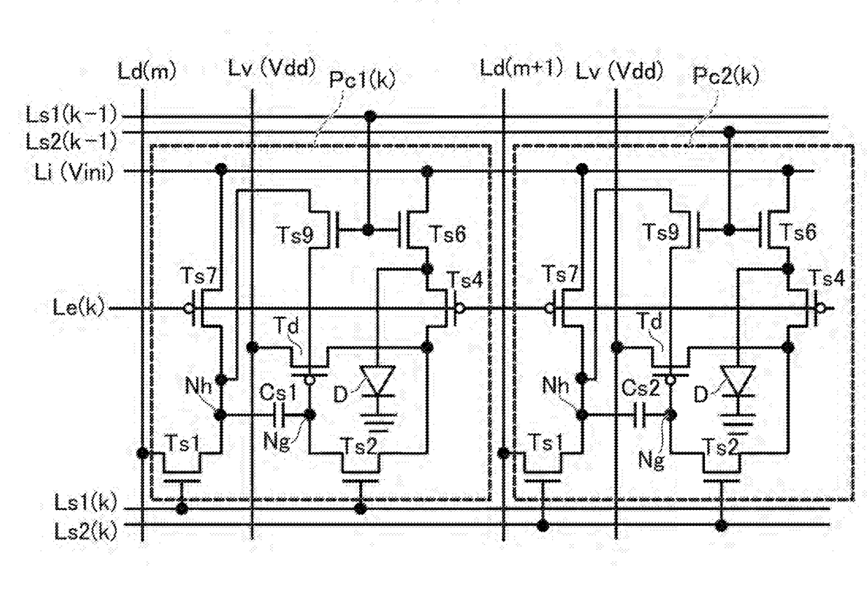
[0031]Hereinafter, embodiments according to the present invention will be described. The disclosure in the present specification is an example of embodiments according to the present invention. Modification that maintain the gist of the present invention are surely contained in the scope of the invention. In addition, a width, a thickness, and a shape of each portion shown in the drawings are an example of the embodiments. The width, the thickness, and the shape shown in the drawings do not limit the interpretation of the invention. The present specification describes, as an example of the display device according to the present invention, an organic EL display having a light emitting element made of an organic electroluminescence material.

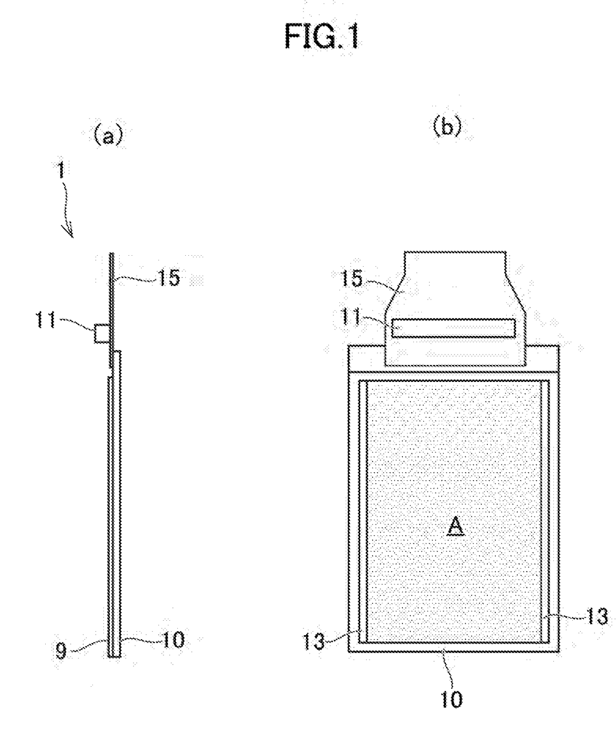
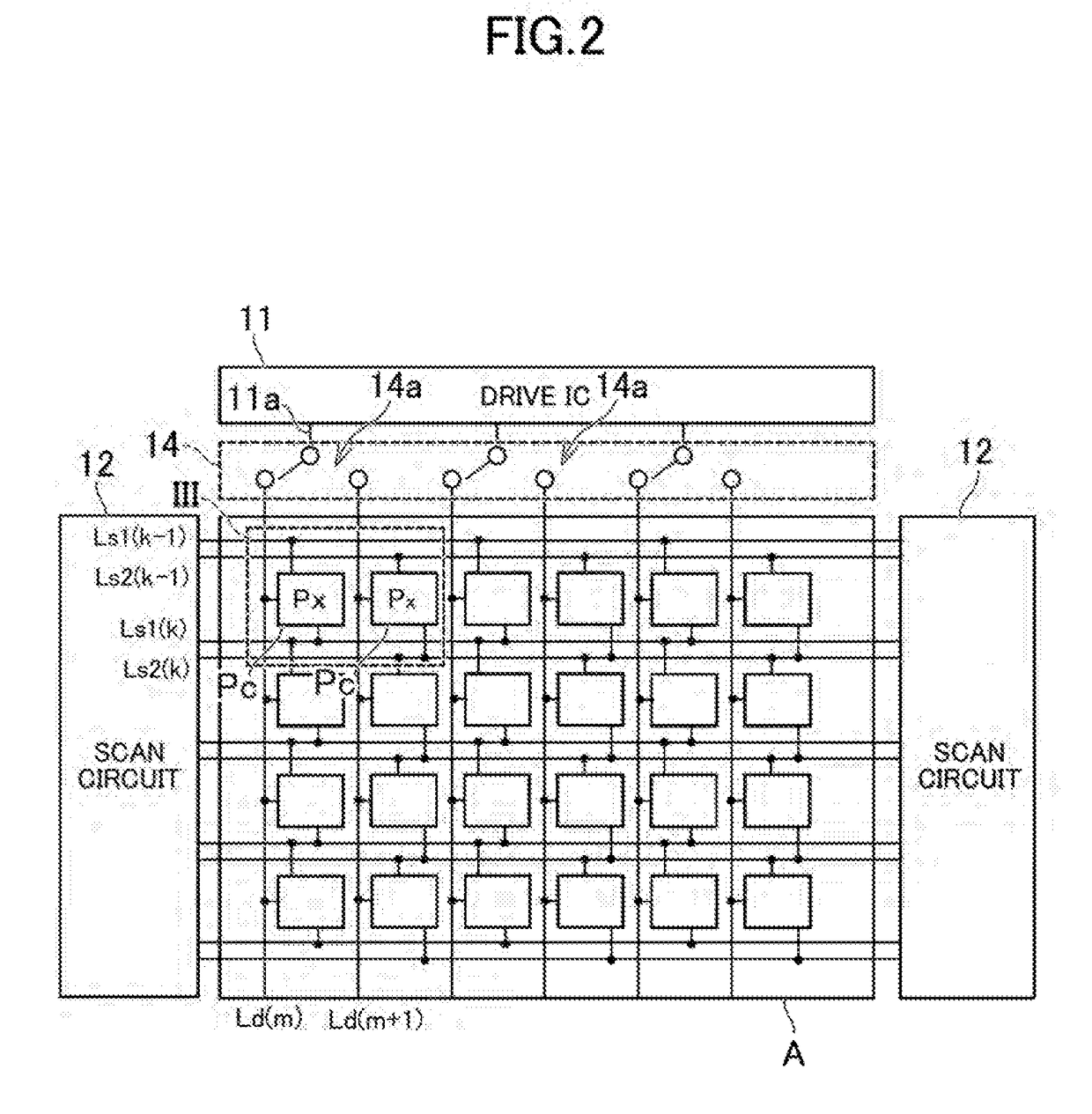
[0032]FIG. 1 shows an organic EL display device 1 according to an embodiment of the present invention. FIG. 1(a) is a side view of the display 1. FIG. 1(b) is a plan view of a substrate 10 of the display device 1. FIG. 2 is for explaining a circui...


PUM


Abstract

In the first signal writing period which is a portion of one horizontal scan period, a first pixel signal is input to the first signal line. The first pixel signal is input from the first signal line to a first pixel circuit throughout a first signal converging period which is longer than the first signal writing period. A second pixel signal is input to the second signal line in a second signal writing period which is another portion of the one horizontal scan period. The second pixel signal is input from the second signal line to a second pixel circuit throughout a second signal converging period which is longer than the second signal writing period. After the first signal converging period and the second signal converging period, electric currents are supplied to the light emitting elements of the first pixel circuit and of the second pixel circuit.

Description

CROSS-REFERENCE TO RELATED APPLICATION[0001]The present application claims priority from Japanese application JP2016-076059 filed on Apr. 5, 2016, the content of which is hereby incorporated by reference into this application.BACKGROUND OF THE INVENTIONField of the Invention[0002]The present invention relates to a display device and a driving method thereof.Description of the Related Art[0003]Organic electroluminescence (EL) displays include, in each pixel, a drive transistor that controls electric current to be supplied to a light emitting element. Differences, among pixels, in threshold voltage Vth of the drive transistor cause inequality in the electric current among pixels to result in uneven brightness in a displayed image. With regard to this problem, some organic EL displays have a countermeasure that compensates the differences, among pixels, in the threshold voltage Vth of the drive transistor. For example, a display device in Japanese Unexamined Patent Application Publicat...

Claims


Application Information

Patent Timeline
Patent Type & Authority Applications(United States)
IPC IPC(8): G09G3/3233G09G3/3266
CPCG09G3/3233G09G3/3266G09G2300/0426G09G2310/0289G09G2310/08G09G3/3275G09G2300/0842G09G2310/0262G09G2310/0297G09G2320/045
Inventor AKIMOTO, HAJIME
Owner JAPAN DISPLAY INC
Why Eureka
Try Eureka