
Power semiconductor device

a technology of power semiconductor and semiconductor chip, which is applied in the direction of semiconductor devices, semiconductor device details, electrical equipment, etc., can solve the problems of limiting the performance of products, large current that reaches several hundred amperes, and time may flow, so as to reduce the transient temperature increase of a power semiconductor chip, increase material cost and device size, and reduce the effect of transient temperature increas

Active Publication Date: 2017-10-05
MITSUBISHI ELECTRIC CORP
View PDF6 Cites 7 Cited by
  • Summary
  • Abstract
  • Description
  • Claims
  • Application Information

AI Technical Summary

Benefits of technology

The present invention aims to provide a power semiconductor device that can prevent the sudden increase in temperature of the semiconductor chip when it is powered. The invention achieves this by using a heat mass that can absorb the heat generated by the semiconductor chip and transfer it to another specific area. This helps to maintain the temperature of the semiconductor device at a safe level without adding any extra materials or increasing the size of the device.

Problems solved by technology

In such equipment, a large amount of current that reaches several hundred amperes in a short time may flow.
In order to prevent trouble or failure in use, product design needs to be based on the thermal resistance at a place in which variation in height is highest, which poses a problem of limiting the performance of the product.
Furthermore, providing the heat diffusion plate poses a problem of increasing the material cost and the module size.
Then, variation in the shape of the solder junction needs to be suppressed, which causes a problem of decreasing the productivity.

Method used


Image

  • Power semiconductor device
  • Power semiconductor device
  • Power semiconductor device

Examples


first embodiment

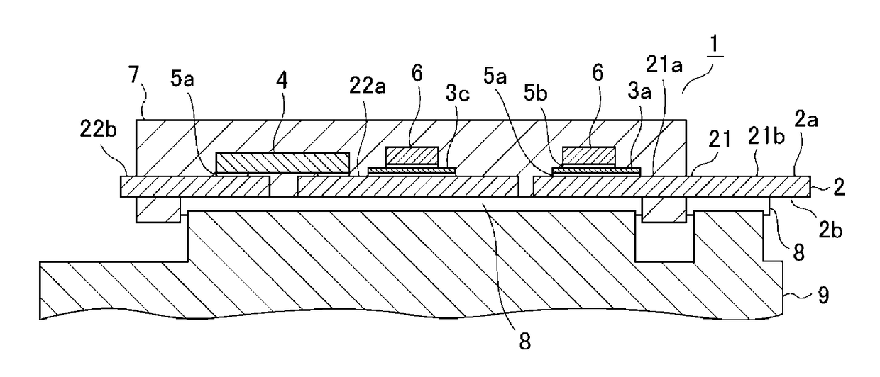
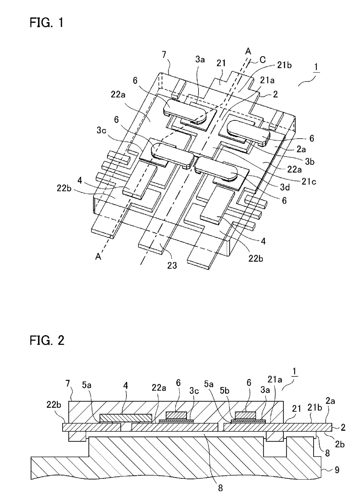
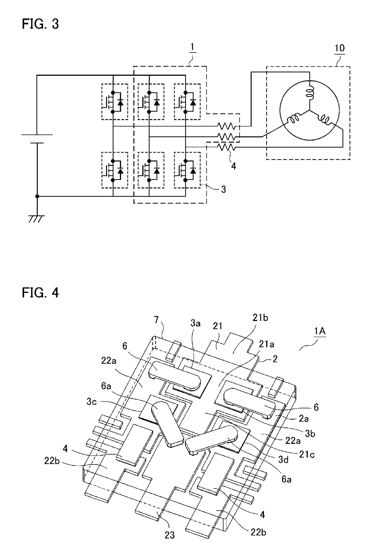
[0020]A power semiconductor device according to a first embodiment of the invention is described below with reference to the drawings. FIG. 1 is an internal perspective schematic view of the power semiconductor device according to the first embodiment. FIG. 2 is a cross-sectional partial view taken along the line A-A in FIG. 1. FIG. 3 is an equivalent circuit diagram of a power conversion circuit including the power semiconductor device according to the first embodiment. Note that, through the drawings, the same or corresponding components are denoted by the same reference numerals.

[0021]A power semiconductor device 1 according to the first embodiment includes: a metallic lead frame 2 shaped in a wiring pattern; switchable upper-side power semiconductor chips 3a, 3b and lower-side power semiconductor chips 3c, 3d (collectively referred to as a power semiconductor chip 3); a current detection resistor 4; conductive joining members 5a, 5b, such as solder; a metallic inner lead 6 as a ...

second embodiment

[0054]FIG. 4 is an internal perspective schematic view of a power semiconductor device according to a second embodiment of the invention. In a power semiconductor device 1A according to the second embodiment, the lower-side power semiconductor chips 3c, 3d mounted on the first intermediate potential electrode 22a are connected to the N-potential electrode 23 by an inner lead 6a that is placed diagonally with respect to the centerline C of the lead frame 2 (see FIG. 1). The remaining parts are configured in the same way as the first embodiment with their description omitted.

[0055]In the power semiconductor device 1A, the lower-side power semiconductor chips 3c, 3d joined to the first intermediate potential electrode 22a, the N-potential electrode 23, and the inner lead 6a connecting them have each respective circular joining surface pad (not shown). This allows the inner lead 6a to be placed diagonally with respect to the lower-side power semiconductor chips 3c, 3d.

[0056]With this c...

third embodiment

[0057]FIG. 5 is an internal perspective schematic view of a power semiconductor device according to a third embodiment of the invention. In a power semiconductor device 1B according to the third embodiment, the lower-side power semiconductor chips 3c, 3d joined to the first intermediate potential electrodes 22a, respectively, and the N-potential electrode 23 are connected by one straight inner lead 6b. The remaining parts are configured in the same way as the first embodiment with their description omitted.

[0058]The lower-side power semiconductor chips 3c, 3d mounted on the first intermediate potential electrodes 22a, respectively, can be connected by the one straight inner lead 6b with half the workload of using two inner leads, which improves the productivity. Furthermore, the inner lead 6b is fixed at three points, which reduces positional misalignment between the lower-side power semiconductor chips 3c, 3d mounted on the first intermediate potential electrodes 22a and the inner ...


PUM


Abstract

When a power semiconductor device is energized, heat generated from upper-side power semiconductor chips mounted on a P-potential electrode transfers to a first heat mass portion and a second heat mass portion, and heat generated from lower-side power semiconductor chips mounted on a intermediate potential electrode transfers to a resistor. A lead frame, the power semiconductor chip, an inner lead and the resistor are placed in symmetry with respect to a centerline, which can reduce the difference among the temperature increases of the power semiconductor chips when energized. In this way, transient temperature increase of the power semiconductor chip can be suppressed without adding a new member, such as a heat diffusion plate.

Description

BACKGROUND OF THE INVENTIONField of the Invention[0001]The present invention relates to a power semiconductor device with a switchable power semiconductor chip mounted on a lead frame.Description of the Background Art[0002]A power semiconductor device is configured by mounting a switchable power semiconductor chip on a mount surface of a lead frame shaped in a wiring pattern and sealing them with a mold resin. The power semiconductor device is used as a single unit or a plurality of units in combination in a power conversion circuit that is incorporated into various products including transportation equipment and home electrical appliances.[0003]When energized, the power semiconductor chip generates heat so that a temperature increases. Then, a current flowing in the power semiconductor chip needs to be controlled so that the temperature will not exceed a predetermined allowable temperature. Specifically, suppressing transient temperature increase of the power semiconductor chip whe...

Claims


Application Information

Patent Timeline
Patent Type & Authority Applications(United States)
IPC IPC(8): H01L23/495H01L23/498
CPCH01L23/49568H01L23/49805H01L23/49575H01L23/49582H01L23/4951H01L23/4952H01L23/49513H01L2924/181H01L2224/40245H01L23/3107H01L23/36H01L23/49524H01L23/49541H01L23/49548H01L23/49562H02M7/003H01L2924/00012H01L2924/00H01L2224/00
Inventor FUKASE, TATSUYAKATO, MASAKIFUJITA, MASAHIKOHORITA, MANABU
Owner MITSUBISHI ELECTRIC CORP
Learn More