Unlock instant, AI-driven research and patent intelligence for your innovation.

Array substrate and activation method for TFT elements in array substrate

a technology of array substrate and activation method, which is applied in the field of display, can solve the problems of abnormal or delayed display images, easy delay of known lcd panels, and slow response of display

Active Publication Date: 2018-02-01
WUHAN CHINA STAR OPTOELECTRONICS TECH CO LTD
View PDF0 Cites 0 Cited by
  • Summary
  • Abstract
  • Description
  • Claims
  • Application Information

AI Technical Summary

Benefits of technology

The present invention provides an array substrate and activation method for TFT elements in the array substrate that can quickly activate TFT elements in low temperature environments. The array substrate comprises a shielding metal layer and a TFT layer. By connecting the shielding metal blocks on the shielding metal layer to electricity to heat up the shielding metal blocks for pre-heating the TFT layer, the activation method accelerates the activation of TFT elements in the TFT layer. This method is advantageous for activating TFT elements in array substrate in low temperature environments.

Problems solved by technology

The northern part of China may experience winter as cold as −40° C. The users in these areas, when powering on electronic display, often experience slow response from the display, abnormal or delayed display images.
The known LCD panel is easily delayed when activated in low temperature environment.

Method used


Image

  • Array substrate and activation method for TFT elements in array substrate
  • Array substrate and activation method for TFT elements in array substrate
  • Array substrate and activation method for TFT elements in array substrate

Examples


Embodiment Construction

[0036]To further explain the technical means and effect of the present invention, the following refers to embodiments and drawings for detailed description.

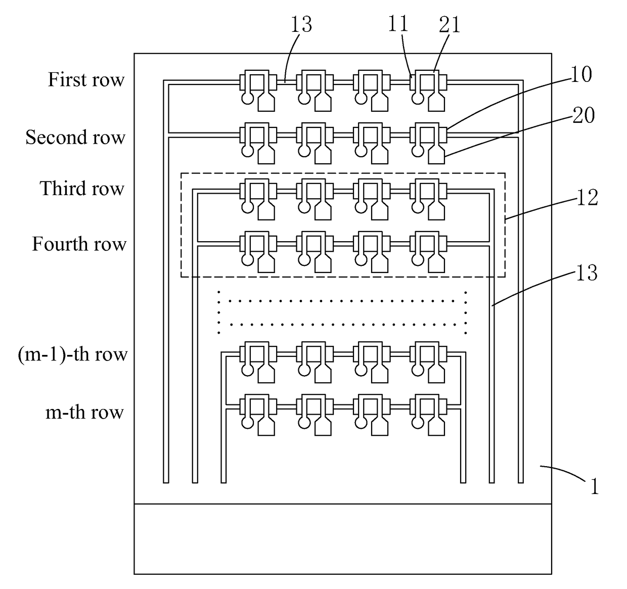
[0037]Refer to FIG. 2. The present invention provides an array substrate, which comprises: a bottom substrate 1, a shielding metal layer 10 disposed on the bottom substrate 1, and a TFT layer 20 disposed on the shielding metal layer 10.

[0038]The shielding metal layer 10 comprises a plurality of shielding metal blocks 11 arranged in a matrix divided into m rows, with the plurality of shielding metal blocks 11 of each row connected through a wire 13.

[0039]In the m rows of shielding metal blocks 11, n rows forms a group, wherein 1≦n≦m, two wires 13 are used to connected respectively the left ends and the right ends of the n rows of shielding metal blocks 11 to form a plurality of parallel combinations 12, so that the two ends of each parallel combination 12 have two outward extending wires 13. By connecting the two wires 13 to a pow...


PUM


Abstract

The invention provides an array substrate and activation method for TFT elements in the array substrate. The array substrate comprises a shielding metal layer (10) and a TFT layer (20) disposed on the shielding metal layer (10); by connecting the shielding metal blocks (11) on the shielding metal layer (10) to electricity to heat up the shielding metal blocks (11) for pre-heating the TFT layer (20) to accelerate activating the TFT elements in the TFT layer (20). The activation method, by connecting the shielding metal blocks (11) on the shielding metal layer (10) to electricity to heat up the shielding metal blocks (11) for pre-heating the TFT layer (20) before activating the TFT elements in the TFT layer (20), accelerates activating the TFT elements in the TFT layer (20). The method is applicable to activating the TFT elements in array substrate in low temperature environment.

Description

BACKGROUND OF THE INVENTION1. Field of the Invention[0001]The present invention relates to the field of display, and in particular to an array substrate and an activation method for thin film transistor (TFT) elements in array substrate.2. The Related Arts[0002]The thin film transistor (TFT) is the main driving element in the liquid crystal display (LCD) and active matrix organic light-emitting diode (AMOLED) display, and is directly related to the development trend of the high performance tablet displays.[0003]The low temperature poly-silicon (LTPS) is the latest TFT substrate manufacturing technology, differs from the conventional a-Si technology mainly in that the LPTS display has the advantages of fast response, high luminance, high resolution and low energy-consumption.[0004]The northern part of China may experience winter as cold as −40° C. The users in these areas, when powering on electronic display, often experience slow response from the display, abnormal or delayed displa...

Claims


Application Information

Patent Timeline
IPC IPC(8): H01L23/34H01L29/786H01L27/12
CPCH01L23/345H01L27/1222H01L27/124H01L27/1255H01L29/78672H01L29/78633G02F1/1368G02F2202/104G02F1/133382G02F1/136209G02F1/1362
Inventor LI, YAFENGPENG, XIANGYI
Owner WUHAN CHINA STAR OPTOELECTRONICS TECH CO LTD
Features
  • R&D
  • Intellectual Property
  • Life Sciences
  • Materials
  • Tech Scout
  • Unparalleled Data Quality
  • Higher Quality Content
  • 60% Fewer Hallucinations
Learn More