Electric field imaging method

a technology of electric field and imaging method, applied in the direction of fluorescence/phosphorescence, instruments, material analysis, etc., can solve the problems of long time-consuming spatial scanning and high demands for real-time imaging techniques, and achieve the effect of suppressing disturbance to objects

Inactive Publication Date: 2018-04-05
NAT INST OF INFORMATION & COMM TECH
View PDF1 Cites 0 Cited by
  • Summary
  • Abstract
  • Description
  • Claims
  • Application Information

AI Technical Summary

Benefits of technology

[0014]In measurement of an electric field at a surface of an object to be visually observed, a high-frequency electric field distribution at a position closer to the object to be visually observed relative to the detection position of the electric field sensor or at a position corresponding to the surface of the object to be visually observed can be imaged while performing observation from a position slightly away from the surface and suppressing disturbance to the object to be visually observed.

Problems solved by technology

In these techniques, electric fields around various electronic circuits or electronic apparatuses are imaged although spatial scanning takes a long time, and intuitive analysis is applied.
Therefore, demands for a real-time imaging technique are high.

Method used


Image

  • Electric field imaging method
  • Electric field imaging method
  • Electric field imaging method

Examples


specific example 1

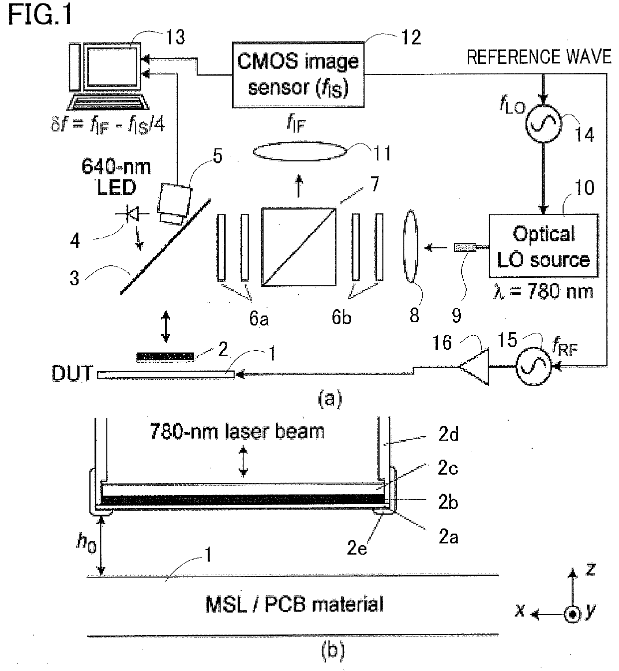
[0054]As a result of trying various M values and hb values to search for a condition where the spatial resolution can be optimally improved, it turned out that M=35 and hb=0.75 mm correspond to h0=0.5 mm. As can be seen in FIG. 7(a) to (c), the spatial resolution is apparently improved. The cause of hb=h0+0.25 mm being an optimum condition is considered to be the holder structure of the electrooptic crystal plate in FIG. 1(b). The influence of the thickness of the electrooptic crystal plate is unknown.

specific example 2

[0055]Even under the condition where h0=0 mm, it is obvious from the above discussion that finite separation substantially exists between the electrooptic crystal plate and the upper surface of the sample. Thus, h0=0 mm is also a target of DEI. When DEI in which hb=0.25 mm was applied to the imaging result of the CRLH line, there was a definite improvement in the spatial resolution (FIG. 7(d)). The electric fields from individual comb-tooth electrodes arranged at an interval of 0.38 mm are clearly separated from one another.

[0056]In this way, a wiring layer surface or an electrode surface, or in a case where there is a dielectric layer covering these surfaces, a surface of the dielectric layer can be applied to the above-described surface.

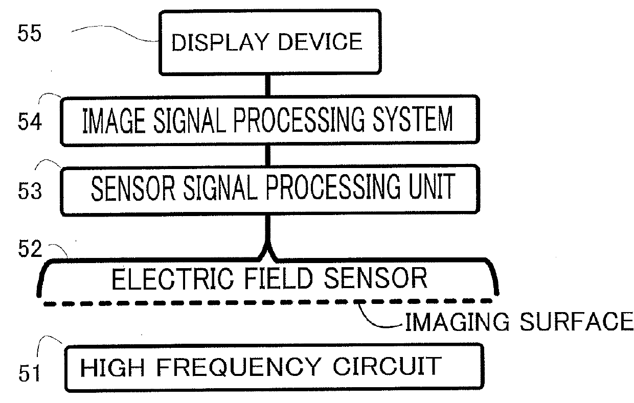
[0057]Also, in a case where a part having a finite height is mounted on a circuit surface or in a case where an electrode is embedded in the circuit surface, a high-definition electric field video image can be obtained in real time, and it is obvio...


PUM

PropertyMeasurementUnit
heightaaaaaaaaaa
heightsaaaaaaaaaa
heightsaaaaaaaaaa

Abstract

To minimize or prevent obstruction by a surface-mounted part or disturbance to an object to be visually observed, an electric field sensor is placed at a predetermined distance from a surface of the object to be visually observed, and a two-dimensional distribution of a high-frequency electric field is detected. Considering that the measured electric field distribution is due to an electrostatic field from the electric field distribution at the surface of the visually observed object, the electric field distribution at the surface is back-calculated from Gauss' flux theorem or the like, and the obtained electric field distribution is displayed or outputted. Thus, the electric field distribution at a position closer to the surface of the visually observed object is imaged while obstruction by a surface-mounted part or disturbance to the visually observed object is suppressed.

Description

TECHNICAL FIELD[0001]The present invention relates to an electric field imaging method for visually observing in real time a spatial evanescent field distribution of a high-frequency signal in an electronic circuit or the like.BACKGROUND ART[0002]Visually observing a spatial distribution of a high-frequency signal of a circuit in real time and intuitively grasping an outline of the operation thereof. This is a function leading to essential innovation, and a method for implementing the function is very attractive from academic and technological viewpoints. Use of the function in various fields, for example, analysis or diagnosis of a high-speed electronic circuit or an advanced antenna, suppression of EMI, and so forth, is expected.[0003]The unique means for visualizing the spatial distribution of the high-frequency signal in real time is the live electrooptic imaging technique, which has been invented by NICT (National Institute of Information and Communications Technology). With th...

Claims


Application Information

Patent Timeline
Patent Type & Authority Applications(United States)
IPC IPC(8): G01N21/552G01R29/08G01N21/64
CPCG01N21/552G01R29/08G01N21/648G01R29/0892
Inventor TSUCHIYA, MASAHIRO
Owner NAT INST OF INFORMATION & COMM TECH
Why Eureka
Try Eureka