Optical sensor

Active Publication Date: 2018-04-19
LITE ON OPTO TECH (CHANGZHOU) CO LTD +1
View PDF8 Cites 10 Cited by
  • Summary
  • Abstract
  • Description
  • Claims
  • Application Information

AI Technical Summary

Benefits of technology

The invention provides an optical sensor that can overcome the issues that were previously present in conventional optical sensors.

Problems solved by technology

However, the carrier of the conventional optical sensor is not formed with a specific structure for guiding the light emitted from the light emitting unit, so that the performance of the conventional optical sensor still leaves much to be desired.

Method used


Image

  • Optical sensor
  • Optical sensor
  • Optical sensor

Examples


first embodiment

[0029]Referring to FIG. 1 to FIG. 3E, a first embodiment of the present disclosure is shown. It should be first noted that relevant quantities and shapes shown in the figures corresponding to this embodiment are only provided to illustrate particular implementations of the present disclosure for ease of understanding, and not to limit the scope of the present disclosure.

[0030]As shown in FIG. 1, FIG. 2A and FIG. 2B, the first embodiment discloses an optical sensor 100, which can be a health sensor, such as: a photoplethysmography (PPG) sensor, but the present disclosure is not limited thereto. The optical sensor 100 in the present embodiment includes a substrate 1, a plurality of light emitting units 2, a frame body 3, an encapsulation 4, and a photodetector 5. The light emitting units 2 and the frame body 3 are disposed on the substrate 1, and the encapsulation 4 encapsulates the light emitting units 2 and the photodetector 5. The specific construction of the optical sensor 100 pro...

second embodiment

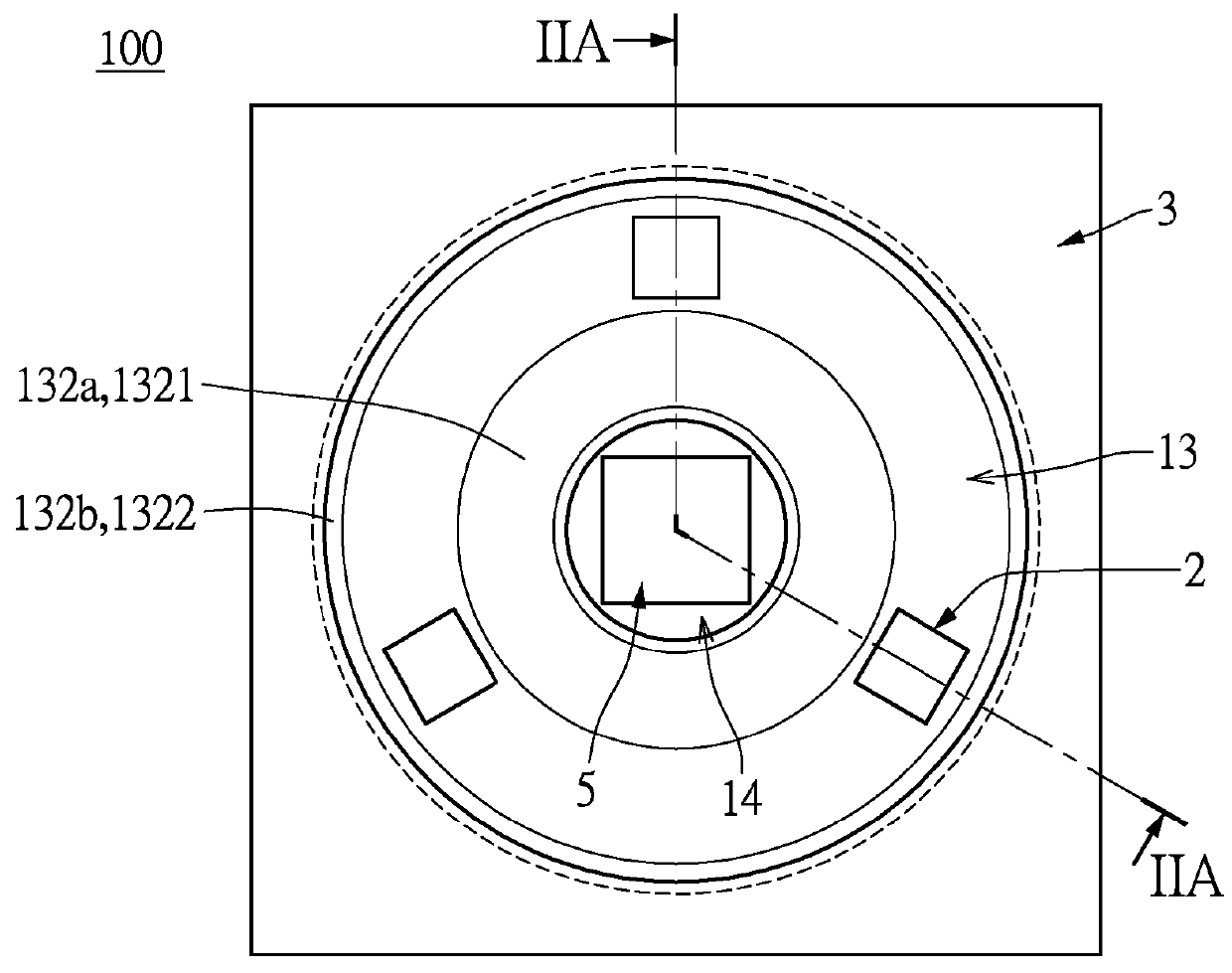
[0046]Referring to FIG. 4 to FIG. 7, a second embodiment of the present disclosure is shown. The second embodiment is similar to the first embodiment, the main differences between the two embodiments being that: in this embodiment, a plurality of receivers 13 are formed in the substrate 1 and a plurality of annular inner wall surfaces 31 are formed in the frame body 3 and corresponding in position to the receivers 13 disposed in the substrate 1. That is, the light guide structure in this embodiment has a plurality of receivers 13 or further a plurality of annular inner wall surfaces 31 of the frame body 3 disposed on corresponding ones thereof.

[0047]Specifically, as shown in FIG. 4 to FIG. 5C, the plurality of receivers 13 are recessed from the first substrate surface 11 of the substrate 1, where the receivers 13 are arranged approximately symmetrically with respect to the preset reference axis C, which overlaps with a central axis of the photodetector 5, and the light emitting unit...

third embodiment

[0055]Referring to FIG. 8 to FIG. 10, a third embodiment of the present disclosure is shown. It should be first noted that relevant quantities and shapes shown in the figures corresponding to this embodiment are only provided to illustrate particular implementations of the present disclosure for ease of understanding, and not to limit the scope of the present disclosure.

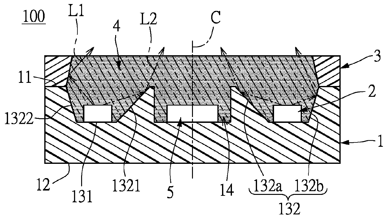
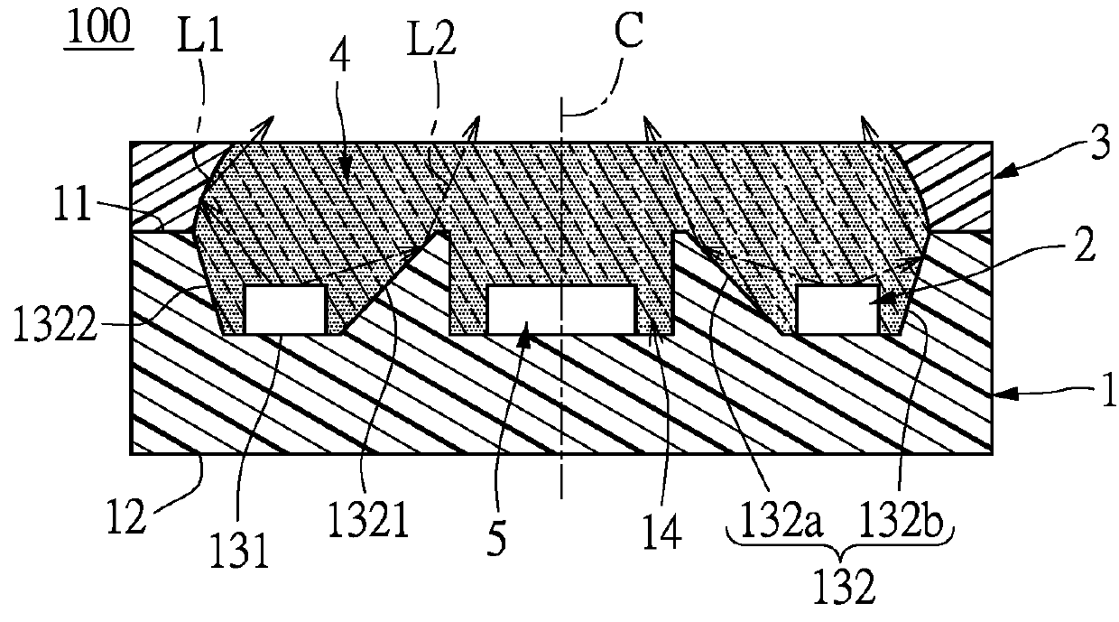
[0056]Moreover, the third embodiment is similar to the second embodiment, the main difference between the two embodiments being the structure of the substrate 1.

[0057]As shown in FIG. 8 and FIG. 9A, the optical sensor 100 includes a substrate 1, a light emitting unit 2, and a photodetector 5. The substrate 1 in the present embodiment is formed with a receiver 13 and a slot 14 both recessed from the first substrate surface 11, and the receiver 13 is located at one side of the slot 14. The structure of the receiver 13 in the present embodiment is similar to that of the second embodiment, but the angle θ1 defined by the...


PUM


Abstract

An optical sensor includes a substrate, light emitting units for emitting light with different wavelengths, and a photodetector. The substrate has at least one receiver for containing these light emitting units and a slot for containing the photodetector. A light guide structure of the optical sensor can be the receiver with a specific design, so that the light emitted by the light emitting units can be reflected towards a central axis of the photodetector. Thus, when at least one of the light emitting units emits light onto an object, the photodetector can receive the light reflected from the object.

Description

CROSS REFERENCE TO RELATED APPLICATION[0001]This application is a continuation-in-part of U.S. application Ser. No. 15 / 153,317 filed on May 12, 2016 and entitled “LIGHT-EMITTING DISPLAY DEVICE”, now pending.BACKGROUND OF THE INVENTION1. Field of the Invention[0002]The present invention relates to a sensor, and in particular, to an optical sensor.2. Description of Related Art[0003]A conventional optical sensor used for health detection includes a carrier, at least one light emitting unit disposed on the carrier, and a photodetector disposed on the carrier for receiving light emitted from the light emitting unit. However, the carrier of the conventional optical sensor is not formed with a specific structure for guiding the light emitted from the light emitting unit, so that the performance of the conventional optical sensor still leaves much to be desired.SUMMARY OF THE INVENTION[0004]The present disclosure provides an optical sensor capable of effectively addressing the potential pro...

Claims


Application Information

Patent Timeline
IPC IPC(8): H01L31/167H01L31/0232H01L31/09G01V8/14G01S17/02H04N1/00H01L31/147G01S17/04
CPCH01L31/167H01L31/02327H01L31/09G01V8/14G01S17/026H04N1/00734H01L31/147G03G2215/00616G01V8/20G01S7/4813G01S7/4815G01S17/04
Inventor CHEN, HUNG-JUI
Owner LITE ON OPTO TECH (CHANGZHOU) CO LTD
Why Eureka
Try Eureka