Pixel driving circuit, display substrate and driving method thereof, and display device

a driving circuit and display substrate technology, applied in the field of display technologies, can solve the problems of affecting light emission display, electric current flowing through the oled, and changing the luminance of the oled with time,

Active Publication Date: 2018-05-17
BOE TECH GRP CO LTD +1
View PDF3 Cites 3 Cited by
  • Summary
  • Abstract
  • Description
  • Claims
  • Application Information

AI Technical Summary

Benefits of technology

[0020]In a third aspect, a method for driving the foregoing display substrate, including a light emission phase which includes a touch phase is provided, wherein in the touch phase of the light emission phase, a touch drive signal is applied to second electrodes in the second electrode pattern through the touch signal lines, and the touch driving compensation unit is controlled through the display signal lines to compensate the voltage of the second energy storage end, so as to maintain that electric current generated by the driving unit does not vary with time.

Problems solved by technology

When the cathode is reused as the touch electrode, a touch drive signal needs to be applied to the cathode, which may cause that electric current flowing through OLED changes because the voltage of the touch drive signal varies with time, thereby making luminance of the OLED vary with time and affecting light emission display.

Method used


Image

  • Pixel driving circuit, display substrate and driving method thereof, and display device
  • Pixel driving circuit, display substrate and driving method thereof, and display device
  • Pixel driving circuit, display substrate and driving method thereof, and display device

Examples


first embodiment

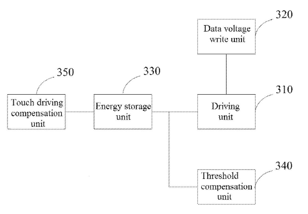
[0035]FIG. 1 is a block diagram of a pixel driving circuit according to the present disclosure. As shown in FIG. 1, the pixel driving circuit of this embodiment may be configured to drive an electroluminescent element, whose cathode is reused as a touch electrode, to display. As shown in FIG. 1, the pixel driving circuit may include a driving unit 310, a data voltage write unit 320, an energy storage unit 330, a threshold compensation unit 340 and a touch driving compensation unit 350. The energy storage unit 330 includes a first energy storage end and a second energy storage end. The driving unit 310 is connected to the first energy storage end to generate a driving current for driving the electroluminescent element connected to the pixel driving circuit according to a difference value between voltage of the first energy storage end and a threshold voltage of the driving unit 310. The data voltage write unit 320 is connected to the driving unit 310 to input data voltage to the driv...

second embodiment

[0072]FIG. 9 is a schematic diagram of a connection relation between a pixel unit and a touch signal line in the display substrate according to the present disclosure. FIG. 9 is a diagram showing connection relation between each second electrode 220 in the second electrode pattern and a touch signal line 400, second electrodes 220 in odd-numbered rows (2n−1, 2n+1 and 2n+3) are interlaced in location with second electrodes 220 in even-numbered rows (2n and 2n+2). In each odd-numbered row, the second electrodes 220 in the same row are connected to a touch signal line 400 in the same row direction. In even-numbered rows, the second electrodes 220 in the same column are connected to a touch signal line 400 in the same column direction. In specific application, when a finger touches any location, electric charges stored on second electrodes 220 (including second electrodes 220 connected to touch signal lines 400 in column direction and second electrodes 220 connected to touch signal line...

third embodiment

[0076]the present disclosure provides a method for driving the foregoing display substrate, and the method includes a light emission phase which comprises a touch phase.

[0077]In the touch phase of the light emission phase, a touch drive signal is applied to second electrodes in the second electrode pattern through the touch signal line, and the touch driving compensation unit is controlled through the display signal line to make driving compensation on the voltage of the second energy storage end, so as to maintain that electric current generated by the driving unit does not vary with time.

[0078]By using the driving method, driving compensation is made on the voltage of the second energy storage end in a touch phase, so that driving current generated by the driving unit 310 does not vary with time. In this way, in the touch phase, luminance of a driven electroluminescent element does not vary with time, thereby avoiding affecting light emission display of the driven electroluminesce...


PUM


Abstract

The present disclosure provides a pixel driving circuit, a display substrate and a driving method thereof, and a display device. The pixel driving circuit includes a driving unit, a data voltage write unit, an energy storage unit, a threshold compensation unit, and a touch driving compensation unit. The energy storage unit comprises a first energy storage end and a second energy storage end. The touch driving compensation unit is connected to the second energy storage end of the energy storage unit to compensate the voltage of the second energy storage end in a touch phase, so as to maintain that driving current generated by the driving unit does not vary with time. The pixel driving circuit provided by the present disclosure can allow luminance of a driven electroluminescent element does not vary with time in a touch phase, thereby avoiding affecting light emission display of the driven electroluminescent element.

Description

CROSS REFERENCE TO RELATED APPLICATIONS[0001]This application is a National Stage Entry of PCT / CN2015 / 098098 filed Dec. 21, 2015, which claims the benefit and priority of Chinese Patent Application No. 201510391775.0 filed Jul. 6, 2015, both of which are incorporated herein by reference in their entirety.BACKGROUND[0002]The present disclosure relates to the field of display technologies, and more particularly, to a pixel driving circuit, a display substrate and a driving method thereof, and a display device.[0003]In one aspect, with respect to an existing display device, an organic light emitting diode (OLED) functioning as a current-mode light-emitting device is increasingly used in the field of high performance display due to its characteristics such as autoluminescence, fast response, wide viewing angle, availability of being fabricated on a flexible substrate, etc. OLED display devices may be classified into two types according to different drive modes, namely, a passive matrix ...

Claims


Application Information

Patent Timeline
Patent Type & Authority Applications(United States)
IPC IPC(8): G09G3/3233G06F3/041
CPCG09G3/3233G06F3/0418G09G2354/00G09G2300/0842G09G2320/0233G06F3/0412G06F3/044G09G2300/0819G09G2300/0861G09G2320/0219G06F3/04184G09G3/32
Inventor YANG, SHENGJIDONG, XUEWANG, HAISHENGCHEN, XIAOCHUANLIU, YINGMINGZHAO, WEIJIEXU, RUIMENG, CHENXUE, JINGDONG, RUIJUNLI, JING
Owner BOE TECH GRP CO LTD
Why Eureka
Try Eureka