
Image-Recognition Processor

a technology of image recognition and processor, applied in the field of integrated circuits, can solve the problems of not only fast memory/storage, but also powerful processor, and the conventional von neumann architecture cannot meet this requirement, and it takes hours to read tb-scale data from a hard drive, let alone processing, etc., to improve the efficiency of rule enforcement, enhance network security, and enhance computer security

Inactive Publication Date: 2018-09-20
HANGZHOU HAICUN INFORMATION TECH
View PDF6 Cites 2 Cited by
  • Summary
  • Abstract
  • Description
  • Claims
  • Application Information

AI Technical Summary

Benefits of technology

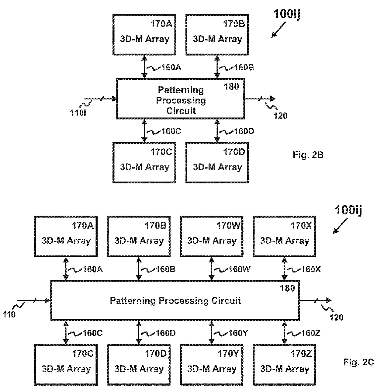
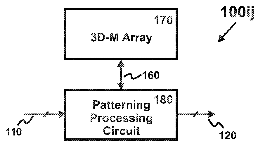
The present invention is a distributed pattern storage-processing circuit that uses three-dimensional memory (3D-M) arrays for both storing and processing patterns. The circuit is housed on a pattern storage-processing die with multiple storage-processing units (SPUs). Each SPU consists of a 3D-M array and a pattern-processing circuit that are communicatively coupled through inter-storage-processor (ISP) connections. The 3D integration of the 3D-M array and pattern-processing circuit offers advantages over conventional 2D integration, including smaller footprint, faster processing, and larger bandwidth. Additionally, the peripheral circuits of the 3D-M arrays can be included without adding much extra cost. Overall, the invention provides a highly efficient and parallel pattern processing solution.

Problems solved by technology

Pattern-processing for such a big database requires not only powerful processor, but also fast memory / storage.
Unfortunately, the conventional von Neumann architecture cannot meet this requirement.
Because a “memory wall” exists between the processor and the memory / storage (i.e. the communication bandwidth between them is limited), it would take hours to even read a TB-scale data from a hard drive, let alone processing it.
This poses as a bottleneck to perform pattern processing for a big pattern database.

Method used


Image

  • Image-Recognition Processor
  • Image-Recognition Processor
  • Image-Recognition Processor

Examples


Embodiment Construction

[0037]Those of ordinary skills in the art will realize that the following description of the present invention is illustrative only and is not intended to be in any way limiting. Other embodiments of the invention will readily suggest themselves to such skilled persons from an examination of the within disclosure.

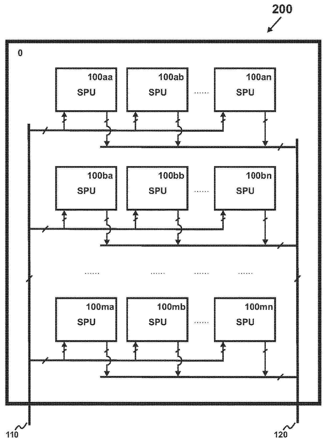
[0038]Referring now to FIG. 1, a preferred pattern storage-processing die 200 is disclosed. It not only stores patterns permanently, but also processes them with massive parallelism. The preferred pattern storage-processing die 200 comprises a distributed pattern storage-processing circuit, which includes an array with m rows and n columns (m×n) of storage-processing units (SPU) 100aa-100mn. Each SPU is commutatively coupled with an input 110 and an output 120. The input 110 includes a first pattern, which could be a network packet, a computer data, a rule pattern, a malware pattern, or the like. In general, the preferred pattern storage-processing die 200 comprises thousan...


PUM


Abstract

A preferred image-recognition processor comprises a plurality of storage-processing units (SPU), with each SPU comprising at least a three-dimensional memory (3D-M) array vertically stacked above a pattern-processing circuit. The 3D-M array stores at least a portion of an image model from an image model database. The image data from the input are sent to all SPUs, which perform pattern recognition simultaneously.

Description

CROSS-REFERENCE TO RELATED APPLICATIONS[0001]This application is a continuation-in-part of application “Distributed Pattern Processor Comprising Three-Dimensional Memory”, application Ser. No. 15 / 452,728, filed Mar. 7, 2017, which claims priorities from Chinese Patent Application No. 201610127981.5, filed Mar. 7, 2016; Chinese Patent Application No. 201710130887.X, filed Mar. 7, 2017, in the State Intellectual Property Office of the People's Republic of China (CN), the disclosures of which are incorporated herein by references in their entireties.[0002]This application also claims priorities from Chinese Patent Application No. 201710460366.0, filed Jun. 17, 2017; Chinese Patent Application No. 201710461244.3, filed Jun. 19, 2017, in the State Intellectual Property Office of the People's Republic of China (CN), the disclosures of which are incorporated herein by references in their entireties.BACKGROUND1. Technical Field of the Invention[0003]The present invention relates to the fiel...

Claims


Application Information

Patent Timeline
Patent Type & Authority Applications(United States)
IPC IPC(8): G06K9/00G06F17/30G06F21/56
CPCG06F17/30256G06F21/566G10L25/51H01L27/249G06F2221/034G06F17/3028H01L27/11578H01L27/1128H01L27/11206G10L15/28G06K9/00986H01L27/11551G06V10/955H10B20/20H10B20/50H10B43/27H10B20/25G06F16/51G06F16/5838H10B41/20H10B43/20H10B63/845
Inventor ZHANG, GUOBIAO
Owner HANGZHOU HAICUN INFORMATION TECH
Learn More