

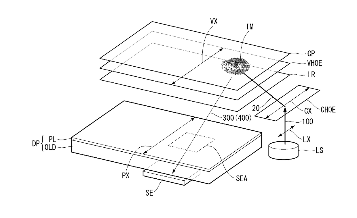
Flat panel display embedding optical imaging sensor
a technology of optical imaging and display screen, which is applied in the direction of identification means, instruments, polarising elements, etc., can solve the problems of limited application of optical fingerprint sensors to various applications such as combining with display devices, using diffused (or diverged) lights having very low directivity, and achieves resolution and sensitivity very high and/or superior
- Summary
- Abstract
- Description
- Claims
- Application Information
AI Technical Summary
Benefits of technology
Problems solved by technology
Method used
Image

Examples
first embodiment
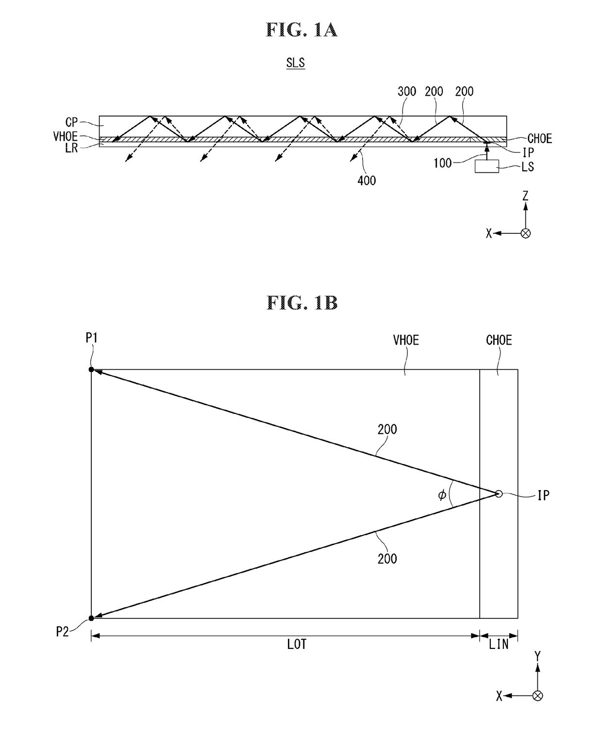
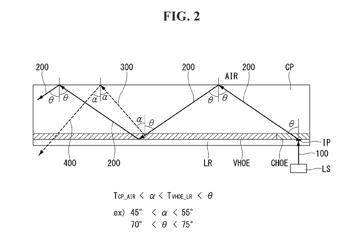
[0035]Hereinafter, referring to FIGS. 1A, 1B and 2, a first embodiment of the present disclosure will be described. FIG. 1A is a drawing illustrating a structure of a directional optical substrate applied for a flat panel display embedding an optical image sensor according to the first embodiment of the present disclosure. In FIG. 1A, the upper drawing is a side view on the XZ plane and FIG. 1B is a plane view on the XY plane.
[0036]Referring to FIGS. 1A and 1B, a directional optical unit according to the first embodiment comprises a directional optical substrate SLS and a light source LS. The directional optical substrate SLS includes a cover plate CP, a light radiating film VHOE, a light incident film CHOE and a low refractive layer LR. The cover plate CP may have a rectangular plate shape of which a length, a width and a thickness. In FIG. 1, the length is along to X-axis, the width is along to Y-axis and the thickness is along to Z-axis.
[0037]The directional optical substrate SLS...
second embodiment
[0081]Hereinafter, referring to FIGS. 5 to 7, we will explain about the second embodiment of the present disclosure. In the second embodiment, the basic structure is very similar with the first embodiment. The differences are like that: in the first embodiment, the directional optical unit has the structure suitable for sensing the image over the large area covering the whole surface of the cover plate as the expanding the propagating lights over the whole surface of the cover plate. In the second embodiment, the directional optical unit has the structure in which the propagating lights are radiated within some restricted image sensing area, and then the image may be reproduced by detecting the reflected lights within the sensing area.
[0082]At first referring to FIG. 5A, we will explain about the directional optical unit according to the second embodiment. FIG. 5A is a drawing illustrating a structure of a directional optical substrate applied for a flat panel display embedding an o...
PUM
| Property | Measurement | Unit |
|---|---|---|
| sizes | aaaaa | aaaaa |
| expanding angle | aaaaa | aaaaa |
| refractive index | aaaaa | aaaaa |
Abstract
Description
Claims
Application Information