
Memristor device and a method of fabrication thereof

Active Publication Date: 2018-12-06
ROYAL MELBOURNE INST OF TECH
View PDF1 Cites 3 Cited by
  • Summary
  • Abstract
  • Description
  • Claims
  • Application Information

AI Technical Summary

Benefits of technology

The present invention provides a method for making a single layer MIM device and a bilayer MIM device that overcome the limitations of conventional STO-based memristor devices. These devices have several benefits that make them more efficient and reliable.

Problems solved by technology

However, the high processing temperatures and non-CMOS compatible substrates typically employed in fabricating STO-based memristor devices can create a barrier to the commercialisation of these devices.

Method used


Image

  • Memristor device and a method of fabrication thereof
  • Memristor device and a method of fabrication thereof
  • Memristor device and a method of fabrication thereof

Examples


Embodiment Construction

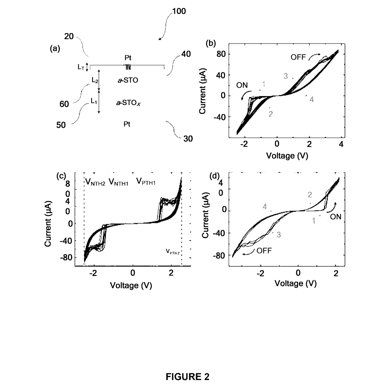
[0051]It should be noted in the following description that like or the same reference numerals in different embodiments denote the same or similar features.

Single Layer Device

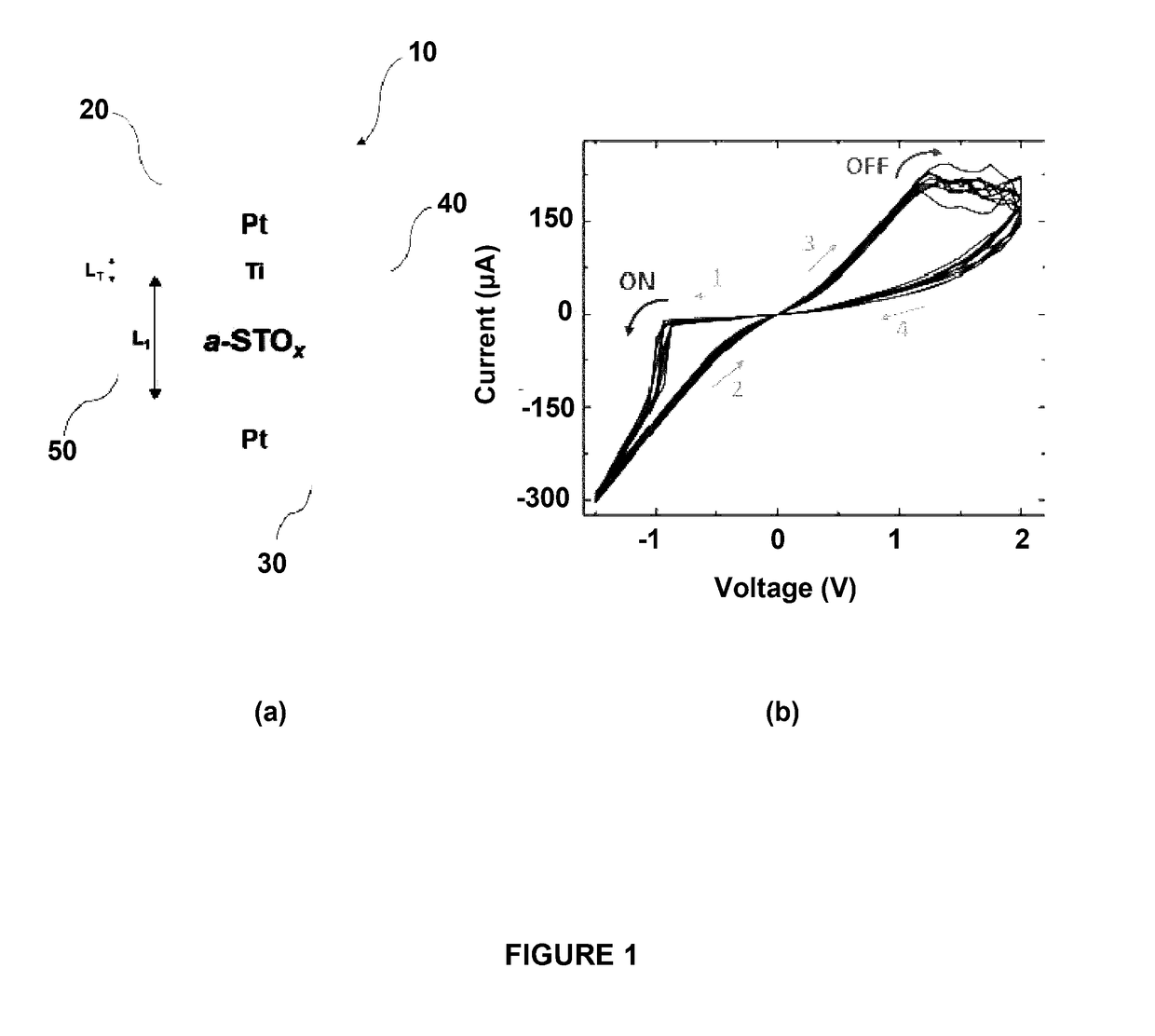
[0052]As shown in FIG. 1(a) there is provided a schematic cross-sectional view of a representative single layer memristor device 10 produced according to a preferred embodiment of the present invention. The single layer device 10 is a stacked passive to terminal metal insulated metal (MIM) device or cell that comprises first and second electrodes 20, 30 that act as the top and bottom electrodes, respectively, of the single layer MIM device 10. The first and second electrodes 20, 30 are inert high work function metal electrodes that are produced from a metal selected from the group consisting of platinum, palladium, gold, tungsten and titanium nitride.

[0053]In a preferred embodiment, the first and second electrodes 20, 30 are formed from platinum metal, each having a thickness that falls within the range of abou...


PUM


Abstract

A memristor device is disclosed comprising: a first electrode; a second electrode; a cathode metal layer disposed on a surface of the first electrode; and an active region disposed between and in electrical contact with the second electrode and the cathode metal layer, the active region comprising at least one layer of an amorphous metal oxide, wherein when a switching voltage is applied between the first and second electrodes, the active region exhibits a resistive switching behaviour. A method of fabricating a memristor device is also disclosed.

Description

TECHNICAL FIELD[0001]The present invention relates to a memristor device and a method of fabrication thereof.[0002]The invention has been developed primarily for use in compatible memristive systems and will be described hereinafter with reference to this application. However, it will be appreciated that the invention is not limited to this particular field of use.BACKGROUND OF INVENTION[0003]The following discussion of the background to the invention is intended to facilitate an understanding of the invention. However, it should be appreciated that the discussion is not an acknowledgement or admission that any of the material referred to was published, known or part of the common general knowledge in Australia or any other country as at the priority date of any one of the claims of this specification.[0004]Memory technologies have traditionally been utilised to store digital data in the form of ones and zeros. Current interest on the other hand, lies in technologies that enable ana...

Claims


Application Information

Patent Timeline
IPC IPC(8): H01L45/00
CPCH01L45/147H01L45/1625H01L45/1253H01L45/08H10N70/24H10N70/826H10N70/8836H10N70/026H10N70/021H10N70/841H10N70/883
Inventor BHASKARAN, MADHUSRIRAM, SHARATHWALIA, SUMEETAHMADABADI, HUSSEIN NILI
Owner ROYAL MELBOURNE INST OF TECH
Learn More