High screen ratio display device with fingerprint identification

a display device and high screen ratio technology, applied in the field of display devices, can solve the problems of inconvenient fingerprint identification for users and fingers stained, and achieve the effect of easy increase of the screen ratio of the display device, high screen ratio, and increased screen ratio

Active Publication Date: 2019-01-03
FOCALTECH ELECTRONICS
View PDF64 Cites 15 Cited by
  • Summary
  • Abstract
  • Description
  • Claims
  • Application Information

AI Technical Summary

Benefits of technology

[0004]The object of the present disclosure is to provide a high screen ratio display device with fingerprint identification, in which an active area of the display device can be further extended downwardly so as to increase the screen ratio, whereby the screen ratio of the display device can be easily increased to exceed a ratio of 16 to 9. Furthermore, by disposing a plurality of sensing electrodes in an area of a thin film transistor array that corresponds to an opening, the display device can be provided with a function of force sensing.

Problems solved by technology

However, as being just beside the finger identification, the camera module 120 is often inadvertently touched at this moment and thus is likely to be stained by the fingers.
Therefore, it is inconvenient for users to perform fingerprint identification in certain usage situations in case of placing the fingerprint identification module 110 on the back side of the mobile phone 100.

Method used


Image

  • High screen ratio display device with fingerprint identification
  • High screen ratio display device with fingerprint identification
  • High screen ratio display device with fingerprint identification

Examples


first embodiment

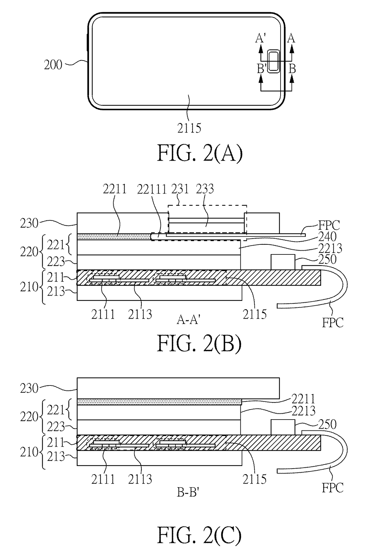
[0026]FIG. 2(A) is a schematic diagram of a high screen ratio display device with fingerprint identification in accordance with the present disclosure. FIG. 2(B) is a cross-sectional view of the display device taken along the A-A′ line in FIG. 2(A). FIG. 2(C) is a cross-sectional view of the display device taken along the B-B′ line in FIG. 2(A). As shown, the high screen ratio display device 200 includes a lower substrate 210, an upper substrate 220 and a cover glass 230.

[0027]The lower substrate 210 has a thin film transistor array 211 and a lower polarizer 213. The thin film transistor array 211 is formed with a plurality of thin film transistors 2111 and corresponding capacitors 2113, by which an active area 2115 is provided on the thin film transistor array 211.

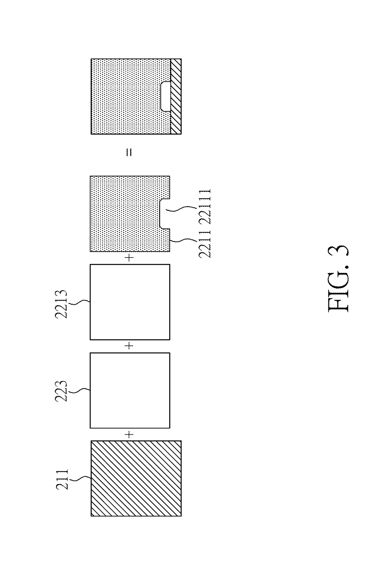
[0028]The upper substrate 220 is disposed on one side of the thin film transistor array 211. The upper substrate 220 includes an optical film layer 221 and a color filter layer 223. The optical film layer 221 includes an ...

second embodiment

[0034]FIG. 4(A) is a schematic diagram of a high screen ratio display device with fingerprint identification in accordance with the present disclosure. FIG. 4(B) is a cross-sectional view of the display device taken along the A-A′ line in FIG. 4(A). FIG. 4(C) is a cross-sectional view of the display device taken along the B-B′ line in FIG. 4(A). As shown, FIGS. 4(A) to 4(C) are similar to FIGS. 2(A) to 2(C) except that the polarizer layer 2213 has a gap 22131 corresponding to the opening 231, so as to define the space 240 in combination with the gap 22111. The gap 22131 is corresponding to the gap 22111; i.e., the position and size of the gap 22131 is the same as those of the gap 22111, while the gap 22131 is located in the polarizer layer 2213 and the gap 22111 is located in the OCA layer 2211.

[0035]FIG. 4(D) schematically illustrates the thin film transistor array, the color filter layer, the polarizer layer and the OCA layer of the display device in accordance with the second emb...

third embodiment

[0036]FIG. 5(A) is a schematic diagram of a high screen ratio display device with fingerprint identification in accordance with the present disclosure. FIG. 5(B) is a cross-sectional view of the display device taken along the A-A′ line in FIG. 5(A). FIG. 5(C) is a cross-sectional view of the display device taken along the B-B′ line in FIG. 5(A). As shown, FIGS. 5(A) to 5(C) are similar to FIGS. 2(A) to 2(C) except that the optical film layer 221 further includes a pad material layer 2215 having a gap 22151 corresponding to the opening 231, so as to define the space 240 in combination with the gap 22111. The gap 22151 is corresponding to the gap 22111; i.e., the position and size of the gap 22151 is the same as those of the gap 22111, while the gap 22151 is located in the pad material layer 2215 and the gap 22111 is located in the OCA layer 2211.

[0037]FIG. 5(D) schematically illustrates the thin film transistor array, color filter layer, polarizer layer, pad material layer and OCA la...


PUM

PropertyMeasurementUnit
areaaaaaaaaaaa
active areaaaaaaaaaaa
optical clearaaaaaaaaaa

Abstract

A high screen ratio display device with fingerprint identification includes a lower substrate, an upper substrate, and a cover glass. The lower substrate has a thin film transistor array formed with a plurality of thin film transistors and corresponding capacitors to provide an active area. The upper substrate is disposed on one side of the TFT array, and has an optical film layer. The cover glass is disposed on one side of the upper substrate, and has an opening to accommodate a fingerprint identification module. The opening at least partially overlaps the active area, and a space is defined between the opening of the cover glass and the thin film transistor array to accommodate a portion of the fingerprint identification module.

Description

BACKGROUND OF THE INVENTION1. Field of the Invention[0001]The present disclosure relates to the technical field of display devices and, more particularly, to a high screen ratio display device with fingerprint identification.2. Description of Related Art[0002]Nowadays, the development trend of mobile phones is moving toward having a high screen ratio, which is from the previous screen ratio of 4 to 3 to the current screen ratio of 16 to 9. For example, the S8 mobile phone sold by Samsung Electronics Inc. has a panel of 5.8 inches and a screen ratio of 18.5 to 9. To obtain a higher screen ratio, the fingerprint identification module is typically designed on the back side of the mobile phone so as not to occupy the front screen of the panel.[0003]FIG. 1 is a schematic diagram of a prior mobile phone. As shown, the fingerprint identification module 110 is placed on the back side of the mobile phone 100 and beside the camera module 120. Users have to use their fingers to touch the finge...

Claims


Application Information

Patent Timeline
Patent Type & Authority Applications(United States)
IPC IPC(8): G02F1/1333G06K9/00H01L27/32G06F3/041
CPCG02F1/13338G06F3/0414H01L27/3248G06K9/00087G06F2203/04105G06V40/1329G06V40/1318G06V40/1365H10K59/123
Inventor HSIAO, PEI-HUNG
Owner FOCALTECH ELECTRONICS
Why Eureka
Try Eureka