Display device and method of manufacturing the same
- Summary
- Abstract
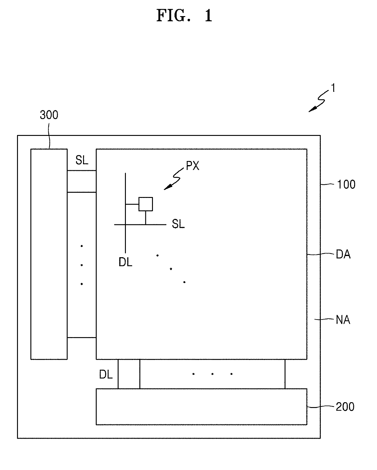
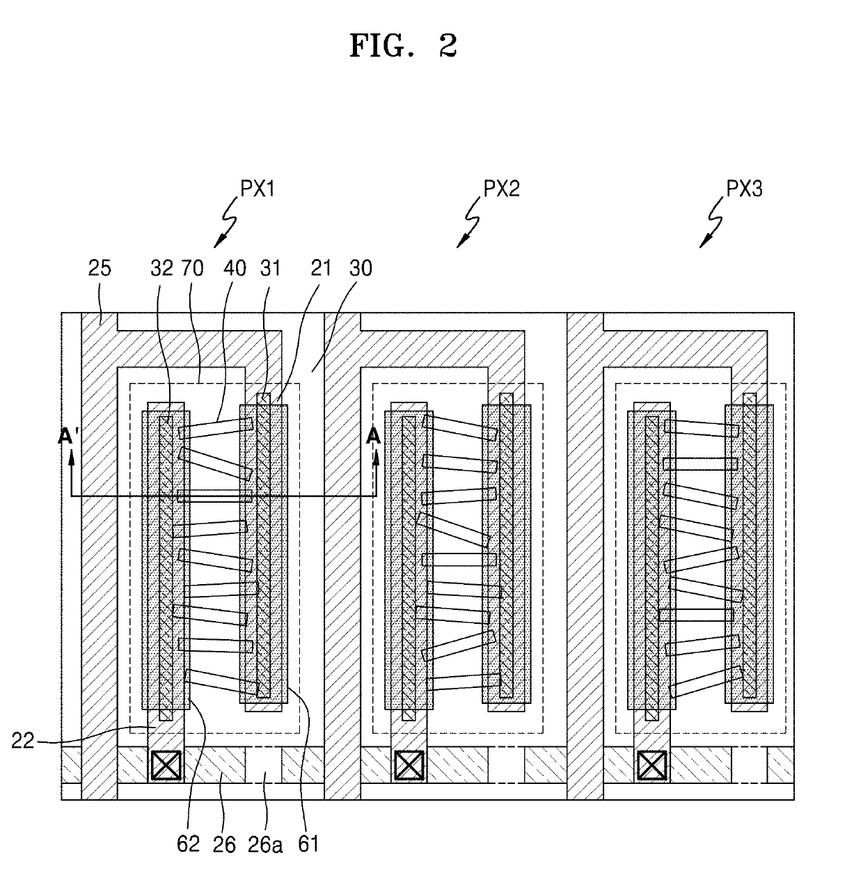
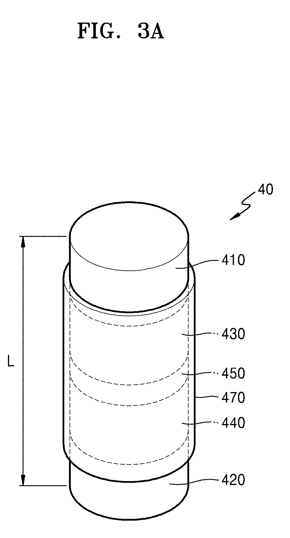
- Description
- Claims
- Application Information
AI Technical Summary
Benefits of technology
Problems solved by technology
Method used
Image

Examples
Embodiment Construction
[0041]As the invention allows for various changes and numerous embodiments, specific embodiments will be illustrated in the drawings and described in detail in the written description. Effects and characteristics of invention, and a method of accomplishing them will be apparent by referring to content described below in detail together with the drawings. However, the illustrated exemplary embodiments are not limited to exemplary embodiments below and may be implemented in various forms.
[0042]Hereinafter, the invention will be described more fully with reference to the accompanying drawings. For clear description of the invention, parts unrelated to descriptions are omitted, and like reference numerals are used for like or corresponding elements and repeated descriptions thereof are omitted when descriptions are made with reference to the drawings.
[0043]It will be understood that when a layer, region, or component is referred to as being “disposed on” another layer, region, or compon...
PUM
 Abstract
Description
Claims
Application Information
 - R&D Engineer
- R&D Manager
- IP Professional
- Industry Leading Data Capabilities
- Powerful AI technology
- Patent DNA Extraction
Browse by: Latest US Patents, China's latest patents, Technical Efficacy Thesaurus, Application Domain, Technology Topic.
© 2024 PatSnap. All rights reserved.Legal|Privacy policy|Modern Slavery Act Transparency Statement|Sitemap