Textured Electrodes with Enhanced Electrochemical Sensitivity

a technology of electrochemical sensitivity and textured electrodes, applied in the field of electrochemical devices, can solve the problems of limited commercialization, non-selective metal deposition, time-consuming, and expensive for translating ideas into functional devices

Active Publication Date: 2019-05-23
MCMASTER UNIV
View PDF0 Cites 7 Cited by
  • Summary
  • Abstract
  • Description
  • Claims
  • Application Information

AI Technical Summary

Problems solved by technology

Though many LOC systems have been developed, the expense and time associated with translating them from a concept to a mass producible LOC device has slowed and limited their commercialization.
While precise control over the deposited film thickness can be achieved with these methods, they are non-selective for metal deposition and need to be combined with additional patterning steps.
Thus, multiple processing steps and expensive vacuum-based instrumentation become necessary, which make these methods complex, expensive, and time-consuming for translating ideas into functional devices.
Direct write printing methods are rapid and inexpensive; however, the resulting electrodes suffer from conductivity issues without high temperature post-printing steps, like sintering, which are often incompatible with many polymer substrates.
Moreover, it is difficult to control the thickness of deposited electrodes, and to create high aspect ratio structures with direct write methods.
While electroless deposition is able to create high quality conductive films, the resulting electrodes lack functional micro- / nano-structure and significant height (>1 μm).

Method used


Image

  • Textured Electrodes with Enhanced Electrochemical Sensitivity
  • Textured Electrodes with Enhanced Electrochemical Sensitivity
  • Textured Electrodes with Enhanced Electrochemical Sensitivity

Examples


example 1

ion Based Process for Making Textured Electrodes

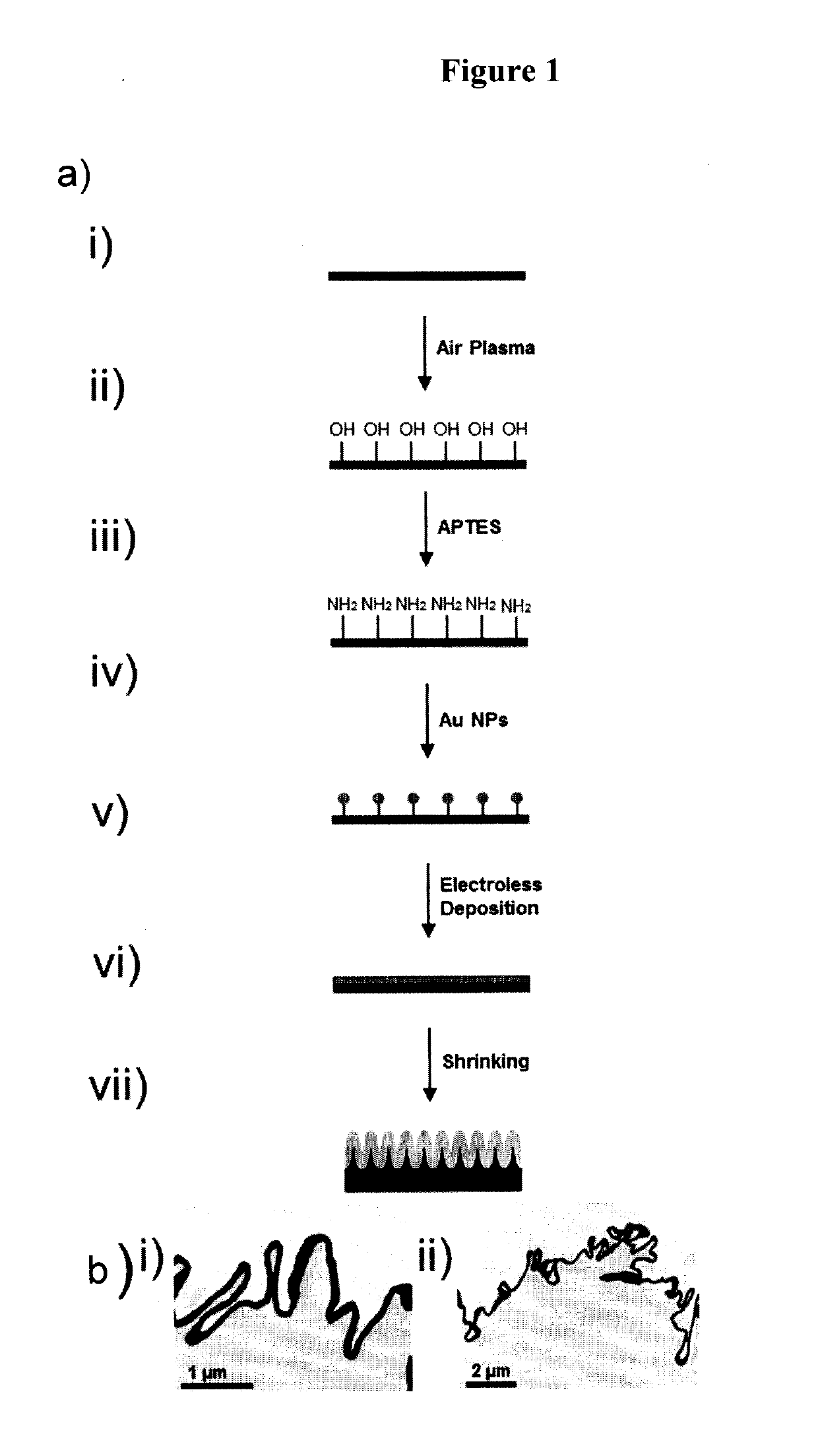
[0042]To address the structural requirements imposed on electrodes that work at the interface between solid-phase devices and solution-phase samples, the following study was conducted to determine whether or not polymer-induced thin film wrinkling methods that have previously been applied solely to sputtered thin films for creating three-dimensional micro / nanostructured structures, could be applied to all-solution-processed films. For this purpose, a fabrication process as schematically represented in FIG. 1 was developed.

[0043]In this method, a clean pre-stressed polystyrene (PS) substrate was treated with air plasma (1 min at 18W RF power) to activate and modify the surface with hydroxyl (—OH) groups (produced during the exposure to air plasma) for subsequent silanization. Then, the activated substrate is incubated in a 10% (3-aminopropyl) triethoxysilane (APTES) solution. The APTES forms a molecular linker (e.g. siloxane linker) for...

example 2

emical Use of Textured Electrodes

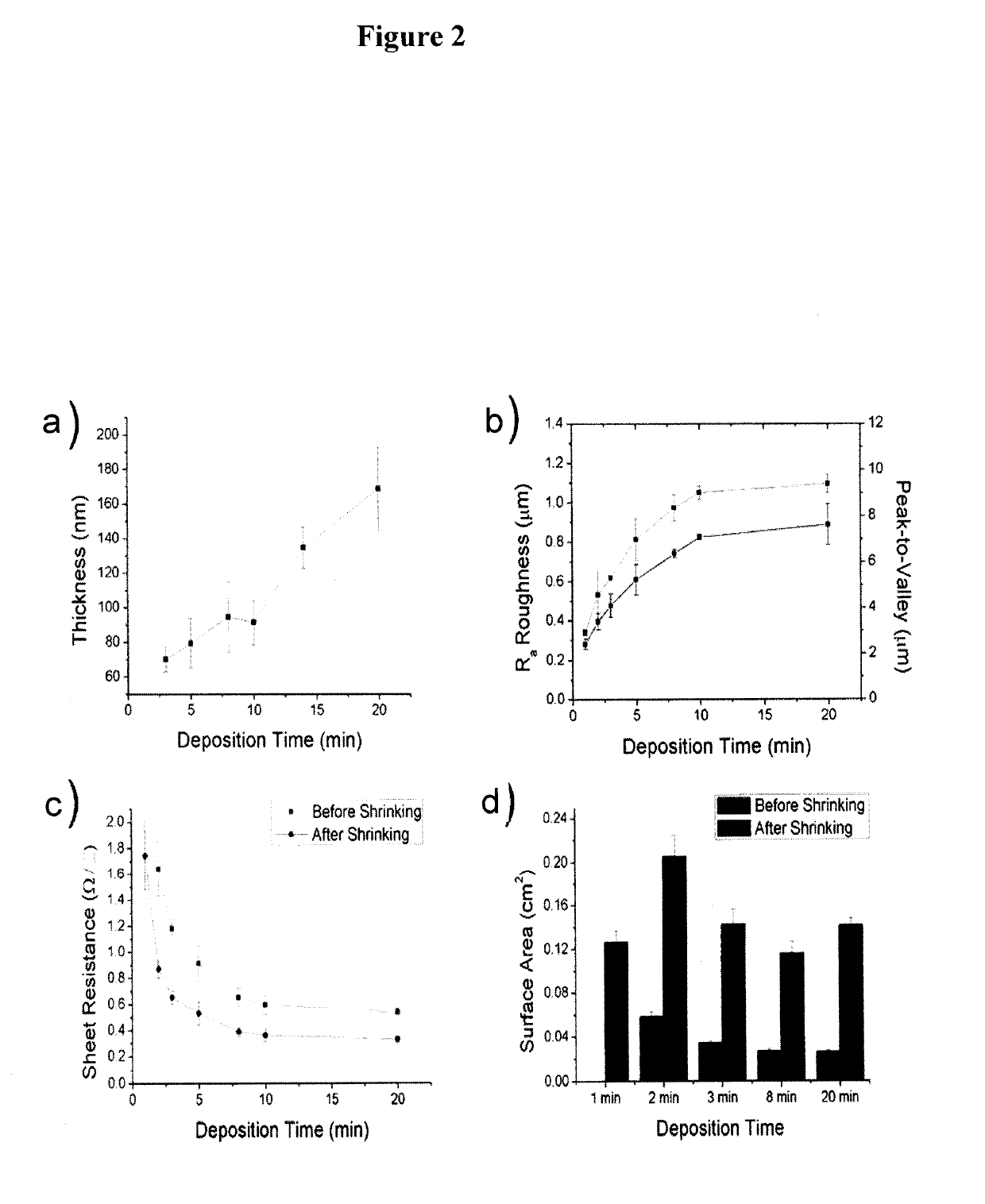
[0054]To assess the suitability of the solution-processed electrodes fabricated as described in Example 1 for use in electrochemical applications and to determine their surface area, electrochemical measurements were conducted for assessing their electroactive surface area (FIG. 2(d)).

[0055]Electrodes deposited for 1 min, 2 min, 3 min, 8 min, and 20 min having the same geometric surface area (0.028 cm2) were evaluated before and after shrinking. The electrochemically-measured surface areas of the electrodes deposited for 8 min and 20 min were approximately equal to their projected surface area before shrinking. However, the measured surface area of the 2 min and 3 min devices were larger by 106% and 20%, respectively, compared to their projected surface areas before shrinking, likely due to the presence of the pores within the electrode film at shorter deposition times. The electroactive surface area of the 1 min before shrinking device could not be ...

example 3

s of Textured Electrodes

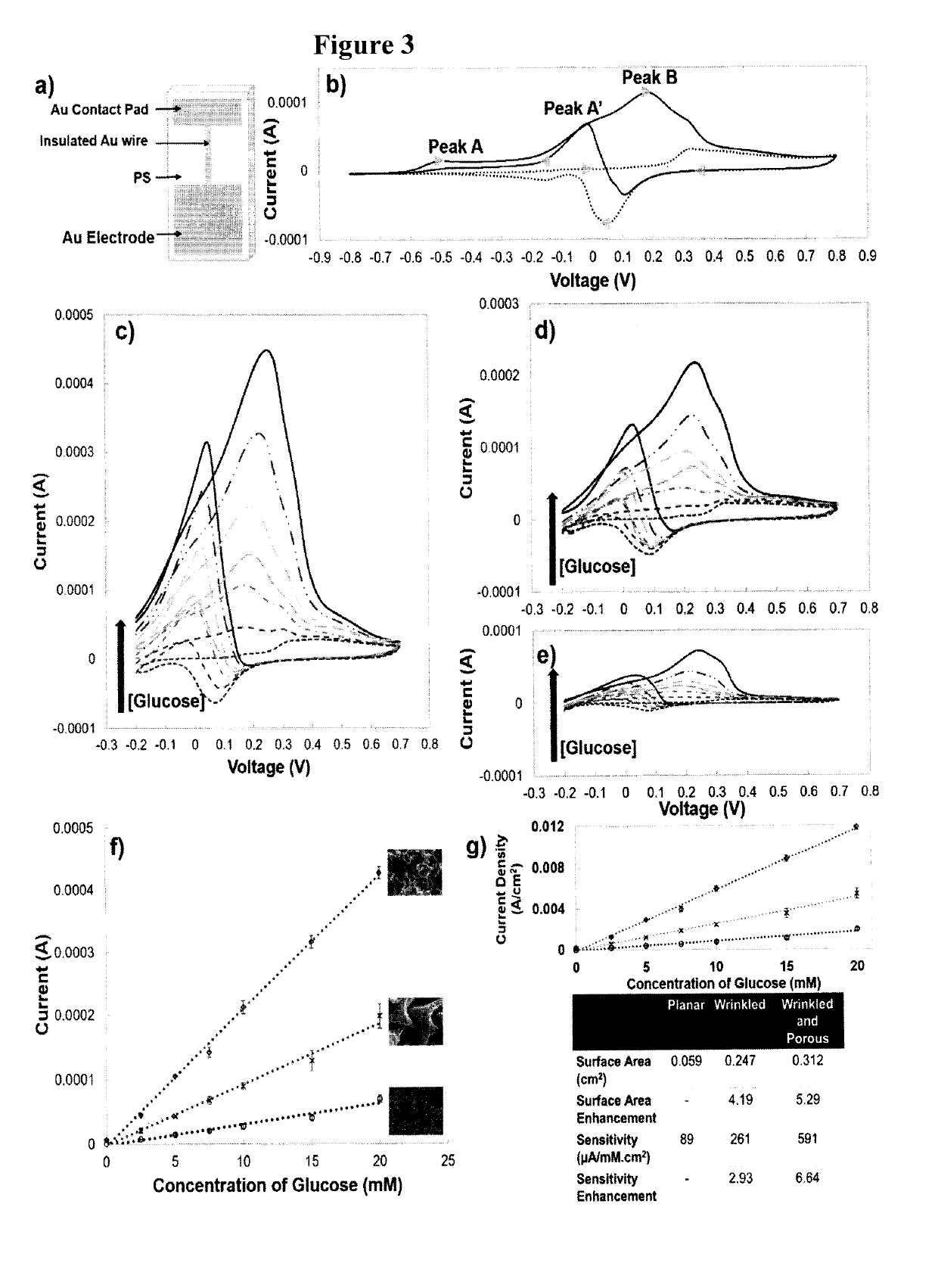
[0057]All-solution-processed sensors that consisted of a wrinkled gold electrode connected to a contact pad through a wire covered by an insulating epoxy were prepared (FIG. 3(a)). The catalytic activity of the wrinkled and porous electrodes (1 min devices) was evaluated by performing cyclic voltammetry (CV) in the presence and absence of glucose in a basic electrolyte (0.1 NaOH). The CV scans presented in FIG. 3(b) demonstrate that in the absence of glucose, gold oxidation starts at ˜0.25 V during the forward scan, and the created gold oxide starts to reduce at ˜0.15 V during the reverse scan. In addition, the redox feature observed at −0.16 V is attributed to the chemisorption of OH− on gold in alkaline solutions. This CV behaviour is in agreement with previously reported Au CV scans in NaOH solutions. In the presence of glucose, the forward scan contains a peak at ˜−0.5 V (peak A), and a broad peak with an onset at ˜−0.2 V that diminishes at ˜0.4 V (peak B...


PUM

PropertyMeasurementUnit
heightaaaaaaaaaa
thicknessaaaaaaaaaa
electro-conductiveaaaaaaaaaa

Abstract

An all-solution electrode fabrication process is provided, The process comprises the steps of: i) preparing and activating a shrinkable polymer substrate for deposition of a a) conductive film; ii) modifying the substrate to incorporate a linker; iii) immobilizing particles of a conductive material on the linkers of the substrate to form a conductive film on the substrate; and vi) heating the modified substrate to a temperature sufficient to cause contraction of the polymer substrate and to result in micro- and / or nano-texturing in the conductive film. The process advantageously yields a novel multi-scale electrode device comprising a polymer substrate; and a textured electro-conductive film linked to the substrate.

Description

FIELD OF THE INVENTION[0001]The present invention generally relates to electrodes, and in particular, to electrodes and methods of fabricating such electrodes for use in electrochemical detection.BACKGROUND OF THE INVENTION[0002]Lab-on-a-chip (LOC) devices for use in point-of care diagnostics have attracted tremendous research and commercial interest over the past two decades. The ability to miniaturize the manual and labor-intensive processing and analytical tasks that are typically performed using large volumes of reagents into integrated and microscale LOC devices is a very attractive and inexpensive alternative to traditional diagnostics systems. Though many LOC systems have been developed, the expense and time associated with translating them from a concept to a mass producible LOC device has slowed and limited their commercialization. Many LOC devices have been fabricated using silicon and glass substrates, however in recent years there has been great interest in using polymer...

Claims


Application Information

Patent Timeline
Patent Type & Authority Applications(United States)
IPC IPC(8): G01N27/327G01N27/30
CPCG01N27/3278G01N27/307G01N27/3277G01N27/30
Inventor GABARDO, CHRISTINESOLEYMANI, LEYLAADAMS-MCGAVIN, ROBERT CHRIS
Owner MCMASTER UNIV
Why Eureka
Try Eureka