Despite significant improvements in individual
cell conversion efficiencies for both
single crystal and thin film approaches, photovoltaic energy collection has been generally restricted to applications having relatively low power requirements.
One factor impeding development of bulk power systems is the problem of economically collecting the energy from an extensive collection surface.
Regardless of whether the cells are
crystalline silicon or thin film, making effective, durable series connections among multiple small cells can be laborious, difficult and expensive.
A first problem which has confronted production of
expansive surface photovoltaic modules is that of collecting the photogenerated current from the top, light incident surface.
These
small cell widths demand very fine interconnect area widths, which dictate delicate and sensitive techniques to be used to electrically connect the top TCO surface of one
cell to the bottom
electrode of an adjacent series connected
cell.
Furthermore, achieving good stable
ohmic contact to the TCO cell surface has proven difficult, especially when one employs those sensitive techniques available when using the TCO only as the top collector
electrode.
One notes that this approach involves use of expensive silver and requires the photovoltaic semiconductors to tolerate the high fusion temperatures.
The
sintering temperatures involved are normally unsuitable for thin film photovoltaic structures.
This wire approach requires positioning and fixing of multiple fine fragile wires which makes
mass production difficult and expensive.
However, the
silver ink approaches require the use of relatively expensive inks because of the required
high loading of finely divided silver.
Furthermore, batch printing on the individual cells is laborious and expensive.
This process is thus laborious, costly and subject to manufacturing error.
Such a process may lead to breaking of electrical connections and complicates efforts to achieve a continuous high volume production process for the integrated cells.
Further, when multiple individual cells are formed monolithically on a common monolithic glass substrate, there is no way to check the quality of individual cells and remove
deficient cell regions.
Thus variations in cell quality over an
expansive surface may jeopardize the entire module.
However, a challenge still remains regarding monolithically subdividing the
expansive films into individual cells followed by interconnecting into a series connected array.
The electrical resistance of thin vacuum metallized
layers may significantly limit the active area of the individual interconnected cells.
Finally, when multiple individual cells are formed on a common monolithic
polymer support film it is difficult to check the quality of individual cells and remove
deficient cell regions.
Thus variations in cell quality over an expansive surface may jeopardize the entire module.
These treatments involve temperatures at which even the most
heat resistant and expensive plastics suffer rapid deterioration.
However, despite the fact that use of a
metal foil allows high temperature
processing in roll-to-roll fashion, the subsequent interconnection of individual cells effectively into an interconnected array has proven difficult, in part because the
metal foil substrate is electrically conducting.
For example, the monolithic integration techniques possible with insulating substrates are not possible using
metal foil substrates, since the common substrate is a conducting metal and would not permit the required
electrical isolation of individual cells prior to electrical series interconnection.
These operations add considerably to the final interconnected array cost.
First, many of the chemical elements involved in the best photovoltaic semiconductors are expensive and environmentally unfriendly.
This removal subsequent to controlled deposition involves containment, dust and
dirt collection and disposal, and possible cell
contamination.
This is not only wasteful but considerably adds to expense since a significant amount of the valuable photovoltaic
semiconductor is lost to the removal process.
Ultimate module efficiencies are further compromised in that the spacing between adjacent cells grows, thereby reducing the effective active collector area for a given module area.
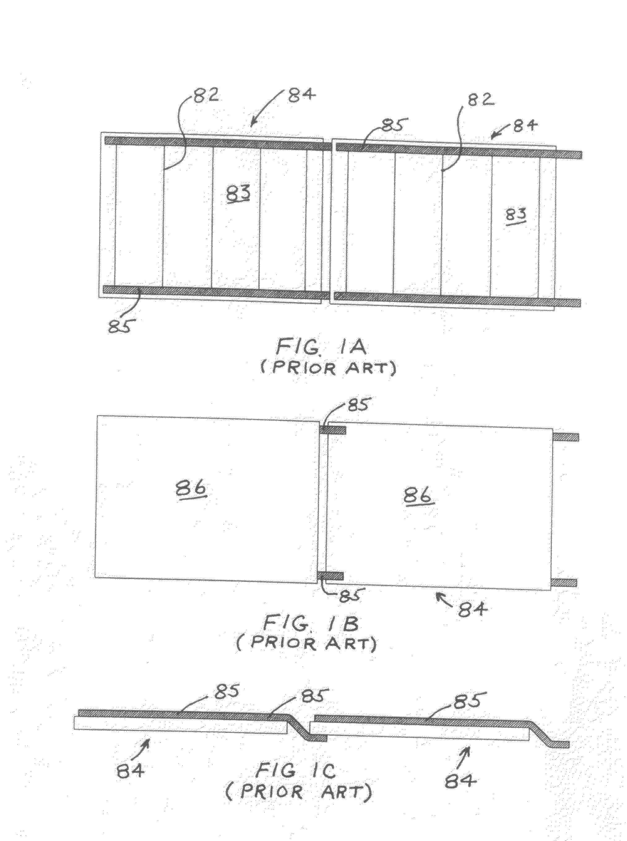
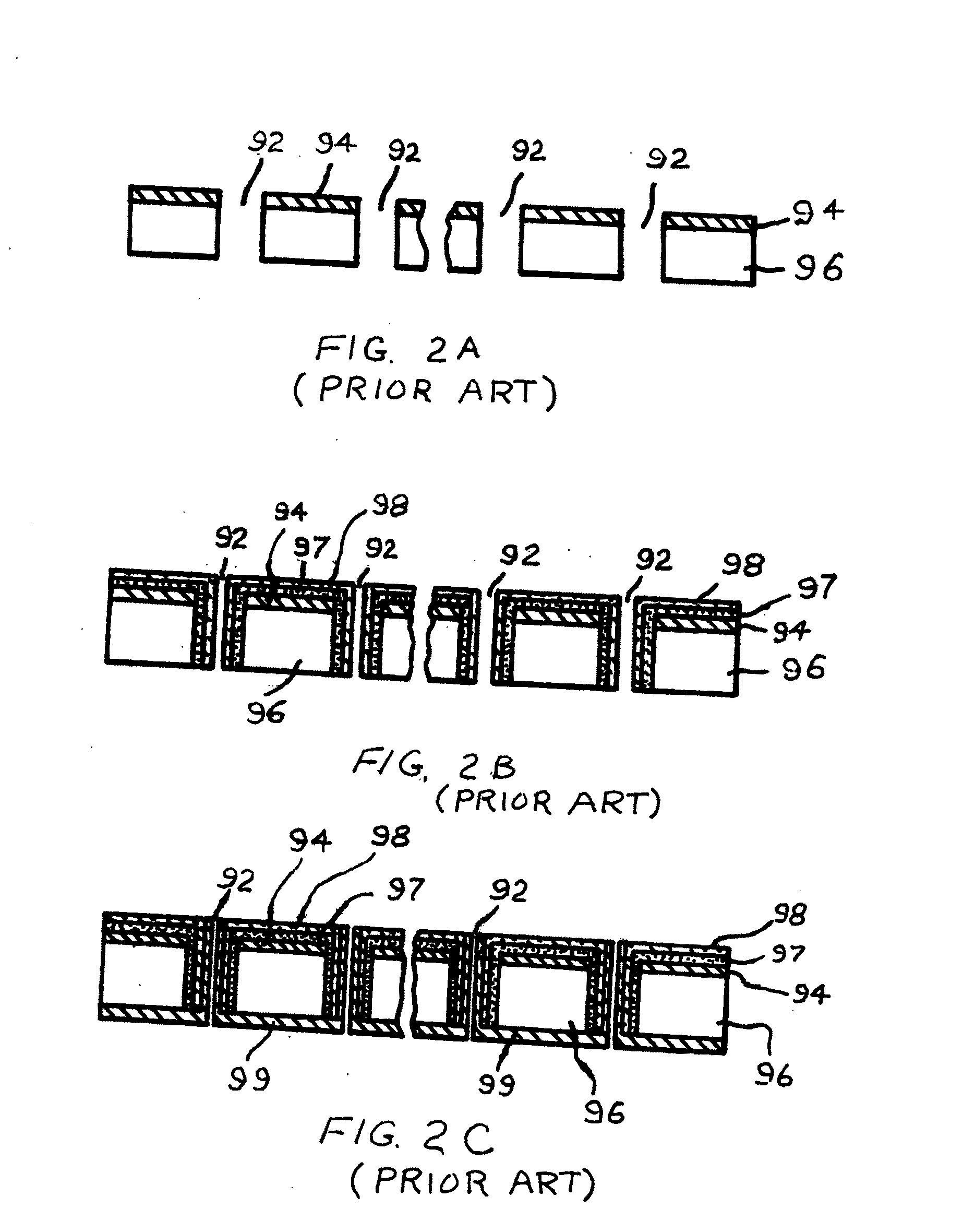
A number of manufacturing and performance problems are intrinsic with the method and structure taught by Yoshida et al.
Vacuum processing is expensive and in practice yields relatively thin deposits.
This relatively low practical thickness limits the current carrying ability of the deposited metal and thereby restricts the size of the individual cells.
While perhaps acceptable when manufacturing
amorphous silicon cells taught by Yoshida et al., it may be unlikely that the films taught would be suitable for the heat treatment requirements of other notable
thin film semiconductors.
The hole density taught by Yoshida et al. is quite large (15 mm centers) adding to complexity.
However, even with the large hole density, the resistive losses expected in current transport to the holes would be quite large given the
sheet resistance of a normal TCO.
There is no way to check the quality of individual cells and remove
deficient cell regions.
Thus variations in cell quality over an expansive surface jeopardize the entire module.
The process is very sensitive to processing variables used to fabricate the plastic substrate, limiting applications to carefully prepared parts and designs.
In addition, the many steps employing harsh chemicals make the process intrinsically costly and environmentally difficult.
Finally, the sensitivity of ABS plastic to
liquid hydrocarbons has prevented certain applications.
This is a misnomer in the strict sense, since ABS (and other nonconductive polymers) are incapable of accepting an electrodeposit directly and must be first metallized by other means before being finally coated with an electrodeposit.
None of these attempts at simplification have achieved any recognizable commercial application.
However, because of
fiber separation (holes) such a composite might not exhibit consistent “microscopic” resistivity.
However, attempts to make an acceptable electroplateable
polymer using the small conductive fillers alone encounter a number of barriers.
First, the most conductive fine metal containing fillers such as silver are relatively expensive.
The loadings required to achieve the particle-to-particle proximity to achieve acceptable
conductivity increases the cost of the polymer / filler blend dramatically.
The metal containing fillers are accompanied by further problems.
They tend to cause deterioration of the mechanical properties and processing characteristics of many resins.
This significantly limits options in resin selection.
A required heavy loading of metal filler severely restricts ability to manipulate processing properties in this way.
A further problem is that metal fillers can be
abrasive to processing machinery and may require specialized screws, barrels, and the like.
Another major obstacle involved in the
electroplating of
electrically conductive polymers is a consideration of adhesion between the electrodeposited metal and polymeric substrate (metal / polymer adhesion).
Despite being
electrically conductive, a simple metal-filled polymer offers no assured bonding mechanism to produce adhesion of an electrodeposit since the metal filler particles may be encapsulated by the resin binder or
oxide, often resulting in a resin-rich or
oxide “
skin”.
For the reasons described above,
electrically conductive polymers employing metal fillers have not been widely used as bulk substrates for electroplateable articles.
An additional obstacle confronting practical
electroplating onto electrically conductive polymers is the initial “bridge” of electrodeposit onto the surface of the electrically
conductive polymer.
However, if the
contact resistance is excessive or the substrate is insufficiently conductive, the electrodeposit current favors the highly conductive member to the point where the electrodeposit will not bridge to the substrate.
Moreover, a further problem is encountered even if specialized
racking or cathodic contact successfully achieves electrodeposit bridging to the substrate.
The conductive polymeric pattern may be relatively limited in the amount of electrodeposition current which it alone can convey.
In a fashion similar to the bridging problem discussed above, the electrodeposition current favors the electrodeposited metal and the lateral growth can be extremely slow and erratic.
This restricts the size and “growth length” of the
conductive ink pattern, increases plating costs, and can also result in large non-uniformities in electrodeposit integrity and thickness over the pattern.
These factors of course often work against achieving the desired result.
A fundamental problem remaining unresolved by the Adelman teaching is the relatively
high resistivity of carbon loaded polymers.
Thus, the electrodeposit bridging and coverage rate problems described above remained unresolved by the Adelman teachings.
Said material addition may have insignificant affect on the current
carrying capacity of the structure (i.e. it does not appreciably reduce resistivity or increase thickness).c. Nevertheless, inclusion of said material greatly increases the speed at which an electrodeposited metal laterally covers the electrically conductive surface.
One or more growth rate accelerators may be present in a directly electroplateable resin (DER) to achieve combined often synergistic results.
Due to multiple performance problems associated with their intended end use, none of the attempts identified above to directly electroplate electrically conductive polymers or plastics has ever achieved any recognizable commercial success.
One readily recognizes that the demand for such functional applications for electroplated articles is relatively recent and has been particularly explosive during the past decade.
Such selective positioning of metals is often expensive and difficult.

