Curved LCD display device

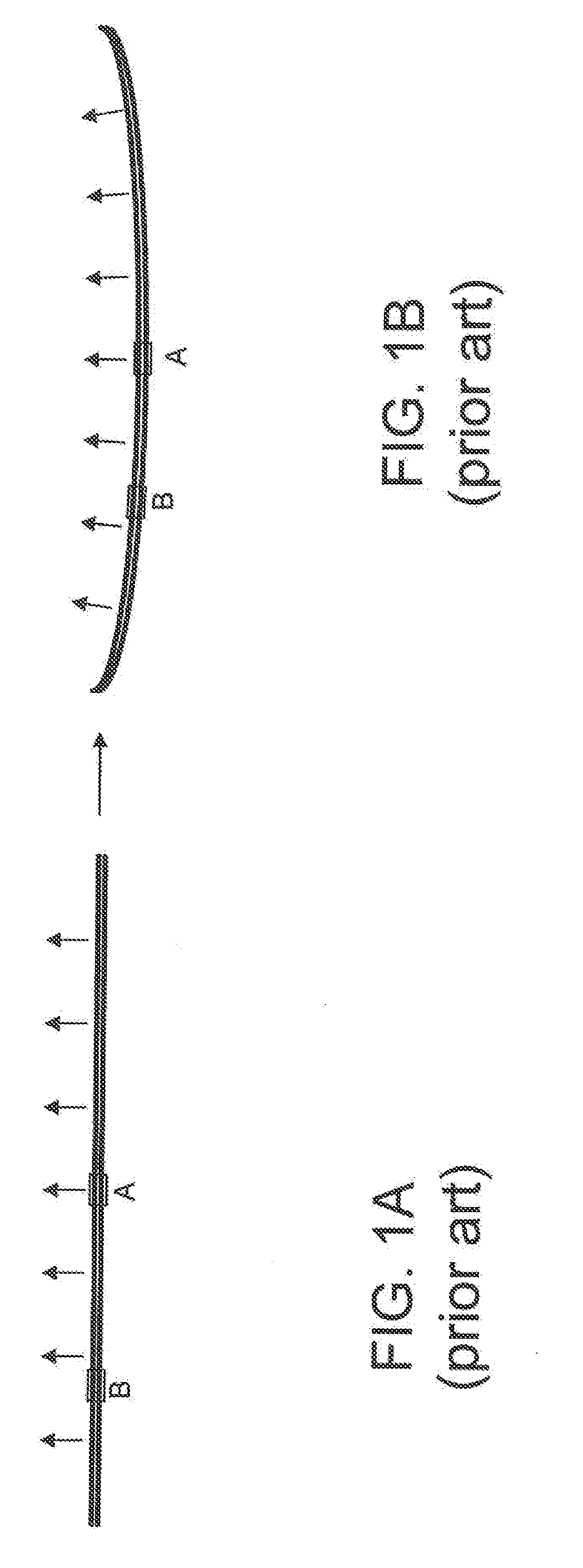
a liquid crystal display and curved technology, applied in semiconductor devices, optics, instruments, etc., can solve the problems of image distortion near the edge and the low contrast ratio based on the viewing angle, the masking element on the cf substrate may not be in perfect alignment with the corresponding opening on the tft substrate, and the corresponding opening may not be in perfect alignment with the corresponding opening, so as to reduce the contrast ratio of the display and improve the contrast ratio

Active Publication Date: 2019-06-06
A U VISTA INC
View PDF12 Cites 0 Cited by
  • Summary
  • Abstract
  • Description
  • Claims
  • Application Information

AI Technical Summary

Benefits of technology

[0007]In a curved liquid crystal, the masking elements on the CF substrate are broader than the bordering areas or openings on the TFT substrate. Thus, each of the aperture areas on the CF substrate is smaller than the corresponding pixel area on the TFT substrate, reducing the contrast ratio of the display. The present invention provides a method and device for improving the contrast ratio in a curved liquid crystal display panel. More specifically, light directing elements with reflective surfaces are arranged between the CF substrate and the TFT substrate to direct part of the light beam transmitted through a pixel area toward the corresponding aperture area.

Problems solved by technology

However, on a large LCD panel, the image distortion near the edge and the low contrast ratio based on the viewing angles become an issue that requires attention.
As a result, the masking element on the CF substrate may not be in perfect alignment with the corresponding opening on the TFT substrate.
For example, while the pixels at location A may have no shift or the shift is negligible (see FIG. 2A), the shift S at location B might result in a substantial misalignment between the masking element and the corresponding opening.

Method used


Image

  • Curved LCD display device
  • Curved LCD display device
  • Curved LCD display device

Examples


Embodiment Construction

[0050]The present invention provides a method and device for improving the contrast ratio in a curved liquid crystal display panel. In particular, the present invention uses a plurality of light directing elements located between the CF substrate and the TFT substrate to effectively condense the light beam transmitted through a pixel area on the TFT substrate. The condensed light beam is arranged to transmit through the aperture on the CF substrate corresponding to the pixel area. As a result, the contrast ratio of the display panel is improved.

FIGS. 3, 4, 5, 5A and 6

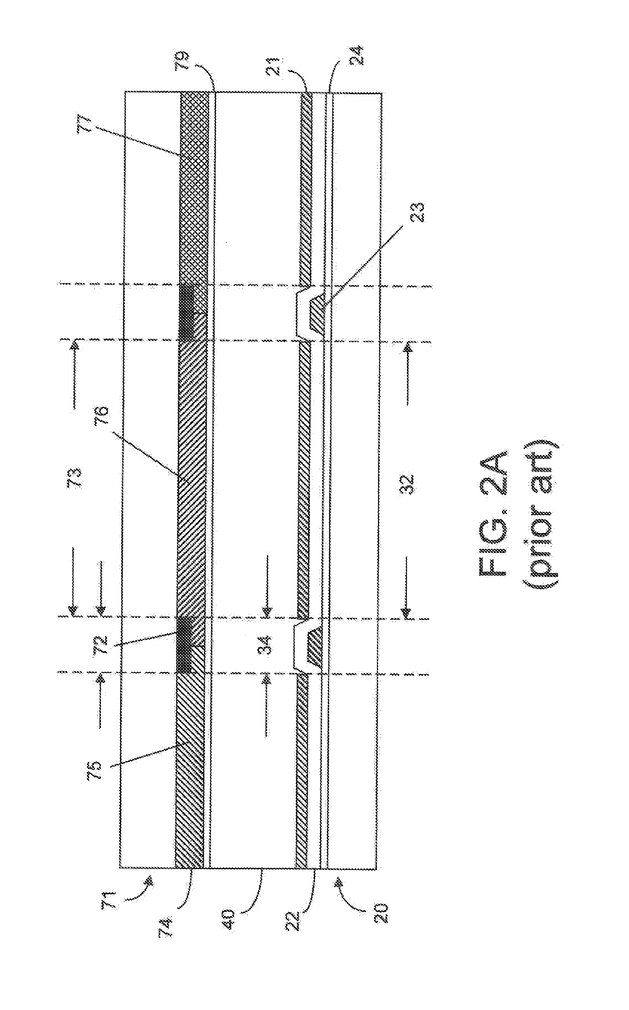
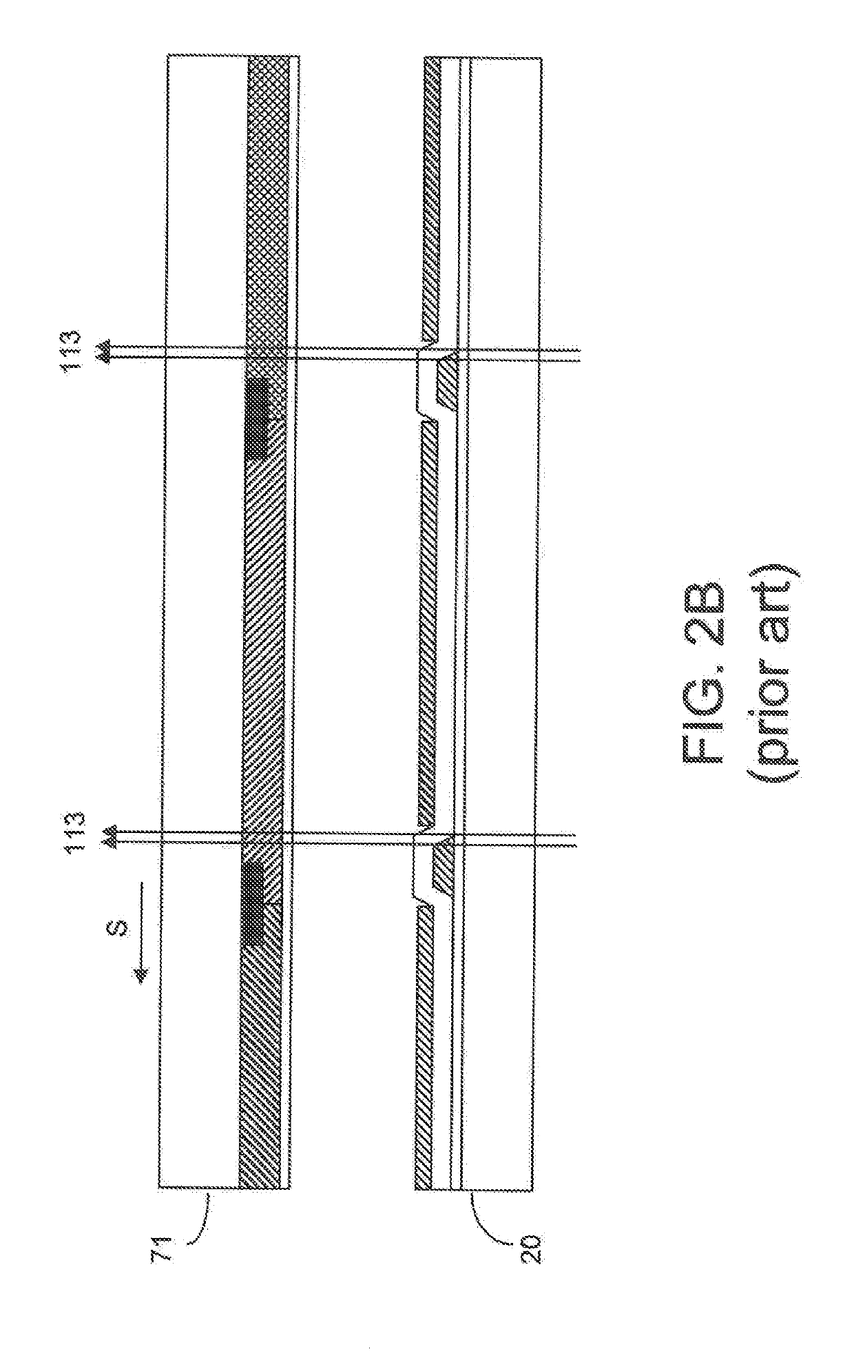
[0051]As shown in FIGS. 3 and 4, the liquid crystal display 10 comprises a first substrate 20, a second substrate 70 and a liquid crystal layer 40 disposed between the first substrate 20 and the second substrate 70. The first substrate 20 comprises a TFT layer 30, which has a plurality of pixel areas 32. The second substrate 70 comprises a color filter layer 60 which comprises a plurality of aperture areas 62 correspond...


PUM

PropertyMeasurementUnit
angleaaaaaaaaaa
angleaaaaaaaaaa
taper angleaaaaaaaaaa

Abstract

A liquid crystal display has a plurality of light directing elements located between the CF substrate and the TFT substrate. The TFT substrate has a plurality of pixel areas and a plurality of bordering areas between adjacent pixel areas. The CF substrate has a plurality of apertures corresponding to the pixel areas and a plurality of masking elements between adjacent aperture areas. Each of the masking elements is broader than the corresponding bordering area on the TFT substrate. The light directing elements with reflective surfaces are used to condense part of the light beam transmitted through a pixel area so as to reduce the beam width of the light beam as it reaches the corresponding aperture. The light directing elements can be located on the CF substrate or the TFT substrate.

Description

TECHNICAL FIELD[0001]The present invention relates generally to a liquid crystal display and, more specifically, to a curved liquid crystal display (LCD) panel.BACKGROUND OF THE INVENTION[0002]LCD TV is capable of delivering on a large screen a realistic, high-image quality viewing experience. However, on a large LCD panel, the image distortion near the edge and the low contrast ratio based on the viewing angles become an issue that requires attention. As a solution, the industry has come up with a curved display panel. A curved LCD panel offers an improved image quality as regard to the image distortion without sacrificing the contrast ratio.[0003]An LCD panel has a CF substrate, a TFT substrate and a liquid crystal layer between the CF substrate and the TFT substrate. As illustrated in FIG. 2A, the TFT substrate 20 has a pixel electrode layer 21, a passivation layer 22, a plurality of data bus lines 23 and a gate insulator layer 24 to form a plurality of pixel areas 32 arranged in...

Claims


Application Information

Patent Timeline
Patent Type & Authority Applications(United States)
IPC IPC(8): G02F1/1333G02F1/1335H01L27/12
CPCG02F1/133308G02F1/133514H01L27/1214G02F1/1333G02F1/133512G02F1/133553G02F1/133565
Inventor LEE, SEOK-LYUL
Owner A U VISTA INC
Why Eureka
Try Eureka