Method of processing wafer

a technology of wafers and die-attaching films, applied in the direction of basic electric elements, electrical apparatus, semiconductor devices, etc., can solve the problems of separating the device chips, difficult to sever the die-attach film at a precise position, and the device chips tend to be out of shap

Active Publication Date: 2019-07-04
DISCO CORP
View PDF5 Cites 6 Cited by
  • Summary
  • Abstract
  • Description
  • Claims
  • Application Information

AI Technical Summary

Benefits of technology

[0007]In the method of processing a wafer according to the aspect of the present invention, after the protective film has been brought into intimate contact with the face side of the wafer including the grooves, the protective film is covered with the liquid resin that is curable by an external stimulus, and then, the liquid resin is cured. The wafer is now fixed to the protective member, preventing the layout of the device chips from varying in subsequent steps such as the step of grinding the reverse side of the wafer. In the method of processing a wafer according to the aspect of the present invention, furthermore, the protective member is peeled off after the die-attach film has been held under suction on the chuck table of the laser processing apparatus. Consequently, since the device chips are kept in position even after the protective member has been removed, the die-attach film can be divided at accurate positions.

Problems solved by technology

However, since the die-attach film is made of a soft material such as a resin, the layout of the device chips tends to be out of shape in a step subsequent to the application of the die-attach film.
If the layout of the device chips varies, it is difficult to sever the die-attach film at a accurate position in a step of eventually separating the device chips.
If this process is performed on a wafer where the layout of device chips has been largely become out of shape, then a processing time required to determine a position where the laser beam is to be applied is likely to be very long.

Method used


Image

  • Method of processing wafer
  • Method of processing wafer
  • Method of processing wafer

Examples


Embodiment Construction

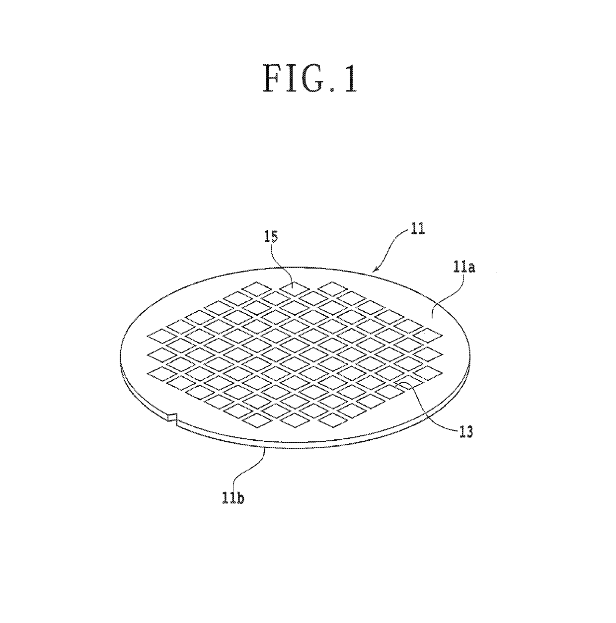
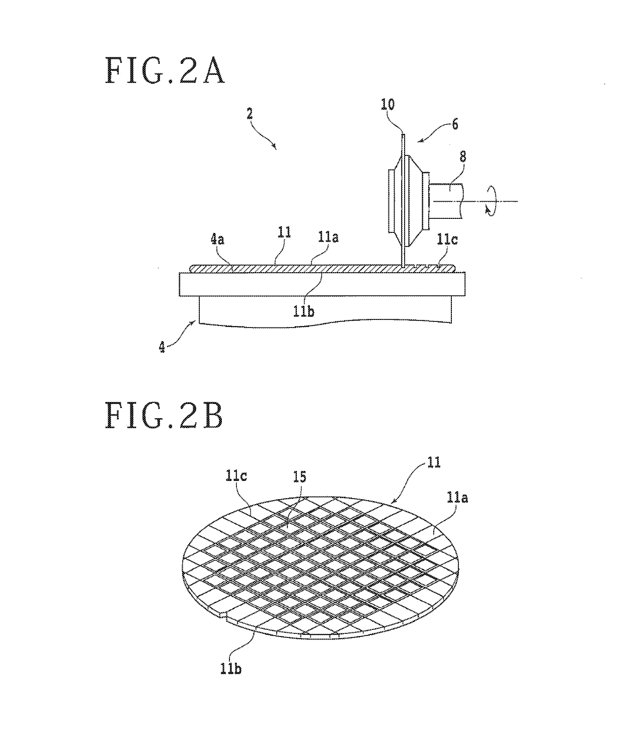
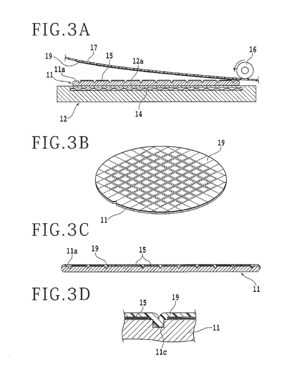
[0028]A method of processing a wafer according to an embodiment of the present invention will be described below with reference to the accompanying drawings. FIG. 1 is a perspective view of a wafer 11 to be processed by the method of processing a wafer according to the present embodiment. As illustrated in FIG. 1, the wafer 11 is of a disk shape having a face side 11a and a reverse side 11b. The wafer 11 may be made of a material such as silicon or the like, for example. The wafer 11 is demarcated into a plurality of areas by a grid of projected dicing lines or streets 13, with a plurality of devices 15 such as ICs (Integrated Circuits) or the like formed respectively in the areas. Though the wafer 11 is illustrated as being of a disk shape and made of silicon or the like in the present embodiment, the wafer 11 is not limited to any materials, shapes, structures, sizes, and so on. Instead, the wafer 11 may be made of materials including semiconductors, ceramics, resins, metals, and ...


PUM


Abstract

A method of processing a wafer having a face side where devices are formed in respective areas demarcated by a grid of projected dicing lines includes a groove forming step, a protective film sticking step, a protective-member-combined wafer forming step, a grinding step, a tape bonding step, a holding step, a peeling step, and a die-attach film dividing step.

Description

BACKGROUND OF THE INVENTIONField of the Invention[0001]The present invention relates to a method of processing a wafer.Description of the Related Art[0002]There has been known a DBG (Dicing Before Grinding) process as a process of manufacturing device chips by dividing a wafer. According to the DBG process, the face side of a wafer where devices are formed is half-cut, and thereafter the reverse side of the wafer is ground, dividing the wafer into device chips. The DBG process is advantageous in that it can restrain chipping of the reverse side of the wafer. In the DBG process, after the wafer has been divided into the device chips by dicing, an adhesive tape called die-attach film is applied to the reverse side of the wafer. The die-attach film is finally divided between the device chips, separating the device chips from each other. Japanese Patent No. 4478053 discloses a method of dividing the die-attach film by applying a laser beam to the die-attach film.SUMMARY OF THE INVENTION...

Claims


Application Information

Patent Timeline
Patent Type & Authority Applications(United States)
IPC IPC(8): H01L21/78H01L21/268H01L21/683
CPCH01L21/78H01L21/268H01L21/6836H01L2221/6834H01L2221/68327H01L2221/68386H01L2221/68377
Inventor SEKIYA, KAZUMA
Owner DISCO CORP
Why Eureka
Try Eureka