Flexible substrate stacking and packaging structure and flexible substrate stacking and packaging method

A technology of flexible substrates and packaging structures, which is applied in the direction of electrical components, electrical solid devices, circuits, etc., can solve problems such as bending circuit layer damage, product stacking failure, etc., to ensure effectiveness and stability, and avoid circuit layer failure Effect

Active Publication Date: 2020-08-28
FOREHOPE ELECTRONICS NINGBO CO LTD
View PDF3 Cites 5 Cited by
  • Summary
  • Abstract
  • Description
  • Claims
  • Application Information

AI Technical Summary

Problems solved by technology

[0003] In the prior art, the IC devices on the flanks of the flexible substrate need to be connected to the circuits on the flanks of the flexible substrate. When bending the flanks, there is a risk of damage to the bent line layer, resulting in failure of the product stack

Method used


Image

  • Flexible substrate stacking and packaging structure and flexible substrate stacking and packaging method
  • Flexible substrate stacking and packaging structure and flexible substrate stacking and packaging method
  • Flexible substrate stacking and packaging structure and flexible substrate stacking and packaging method

Examples


no. 1 example

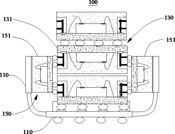
[0056] see in conjunction Figure 1 to Figure 4 , this embodiment provides a flexible substrate stack package structure 100, which is applied to the device package of the flexible substrate, and can avoid the problem of failure of the circuit layer caused by the bending of the flexible substrate 110 while ensuring the number of device stack packages, and ensures the stacking. effectiveness and stability.

[0057] The flexible substrate stack package structure 100 provided in this embodiment includes a flexible substrate 110, a first device package assembly 130 and a second device package assembly 150, the first device package assembly 130 is mounted on the middle of the flexible substrate 110, and is connected to the flexible substrate 110 is electrically connected, and the second device package assembly 150 is insulated and mounted on the side wings of the flexible substrate 110; wherein, the side wings of the flexible substrate 110 are turned upwards so that the second devic...

no. 2 example

[0080] see Figure 5 , an embodiment of the present invention provides a flexible substrate stack packaging method for preparing the flexible substrate stack packaging structure 100 described in the first embodiment, the method includes the following steps:

[0081] S1: Mount the first device package assembly 130 on the middle of the flexible substrate 110 .

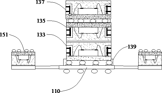
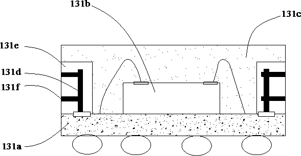
[0082] Specifically, it is necessary to prepare the front-mounted IC devices 131 first, and stack a plurality of front-mounted IC devices 131 in the middle of the flexible substrate 110 in order to form the first device package assembly 130, wherein every two adjacent front-mounted IC devices 131 are reversed. stack.

[0083] In this embodiment, a plurality of positively mounted IC devices 131 includes a first IC device 133, a second IC device 135, and a third IC device 137. When step S1 is performed, the first IC device 133 is first mounted on the flexible substrate 110 and fill the bottom of the first IC device 133 w...


PUM


Abstract

The embodiment of the invention provides a flexible substrate stacking and packaging structure and a flexible substrate stacking and packaging method and relates to the technical field of chip packaging. The flexible substrate stacking and packaging structure and the flexible substrate stacking and packaging method are provided. A second device packaging assembly is attached to a side wing of a flexible substrate; the second device packaging assembly is electrically isolated from the flexible substrate, and the second device is electrically connected with the first device packaging assembly torealize an electrical connection function, thereby avoiding the arrangement of a circuit layer on the flexible substrate, further avoiding the problem of failure of the circuit layer caused by the bending of the flexible substrate, and guaranteeing the effectiveness and stability of stacking.

Description

technical field [0001] The present invention relates to the technical field of chip packaging, in particular to a flexible substrate stack packaging structure and a flexible substrate stack packaging method. Background technique [0002] With the rapid development of the semiconductor industry, the miniaturization of electronic products is getting higher and higher density, more and more functions, the product size is getting smaller and smaller, and the distance between solder balls is getting smaller and smaller. Therefore, POP (Package on Package) stacking structure is widely used in the semiconductor industry. And the combination of flexible substrate stacking structure and POP product stacking, it will stack different functional chips after packaging, the main advantages are high-density integration, small size of packaged products, superior product performance, and large use of stacking space. [0003] In the prior art, the IC devices on the flanks of the flexible sub...

Claims


Application Information

Patent Timeline
Patent Type & Authority Applications(China)
IPC IPC(8): H01L25/07H01L23/31H01L23/498
CPCH01L23/3128H01L23/49816H01L25/071H01L2224/48091H01L2224/48227H01L2924/15311H01L2924/00014
Inventor 何正鸿蒋瑞董
Owner FOREHOPE ELECTRONICS NINGBO CO LTD
Why Eureka
Try Eureka