Cutting method of workpiece
a cutting method and workpiece technology, applied in the direction of semiconductor devices, semiconductor/solid-state device testing/measurement, instruments, etc., can solve the problem of difficult detection of the position of the cut groove overlapping with the laser-processed groove, and achieve accurate detection, prevent damage to the device in the device region, and detect accurately
- Summary
- Abstract
- Description
- Claims
- Application Information
AI Technical Summary
Benefits of technology
Problems solved by technology
Method used
Image

Examples
Embodiment Construction
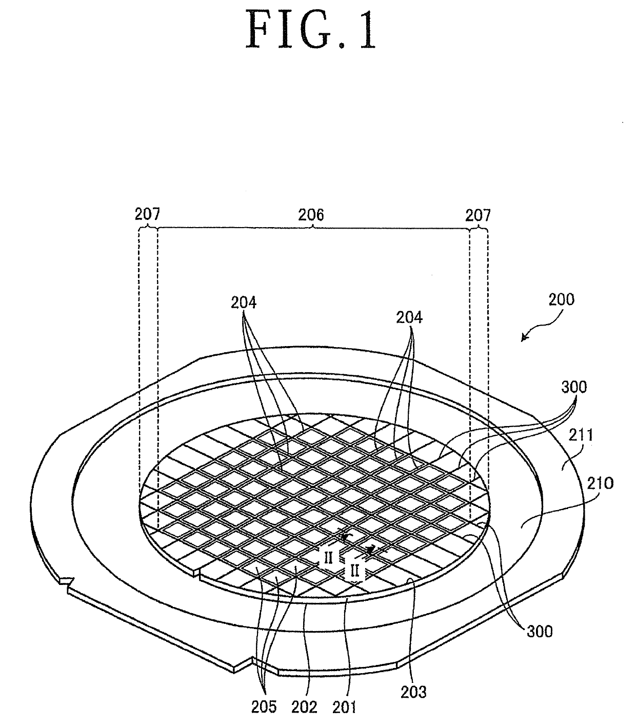
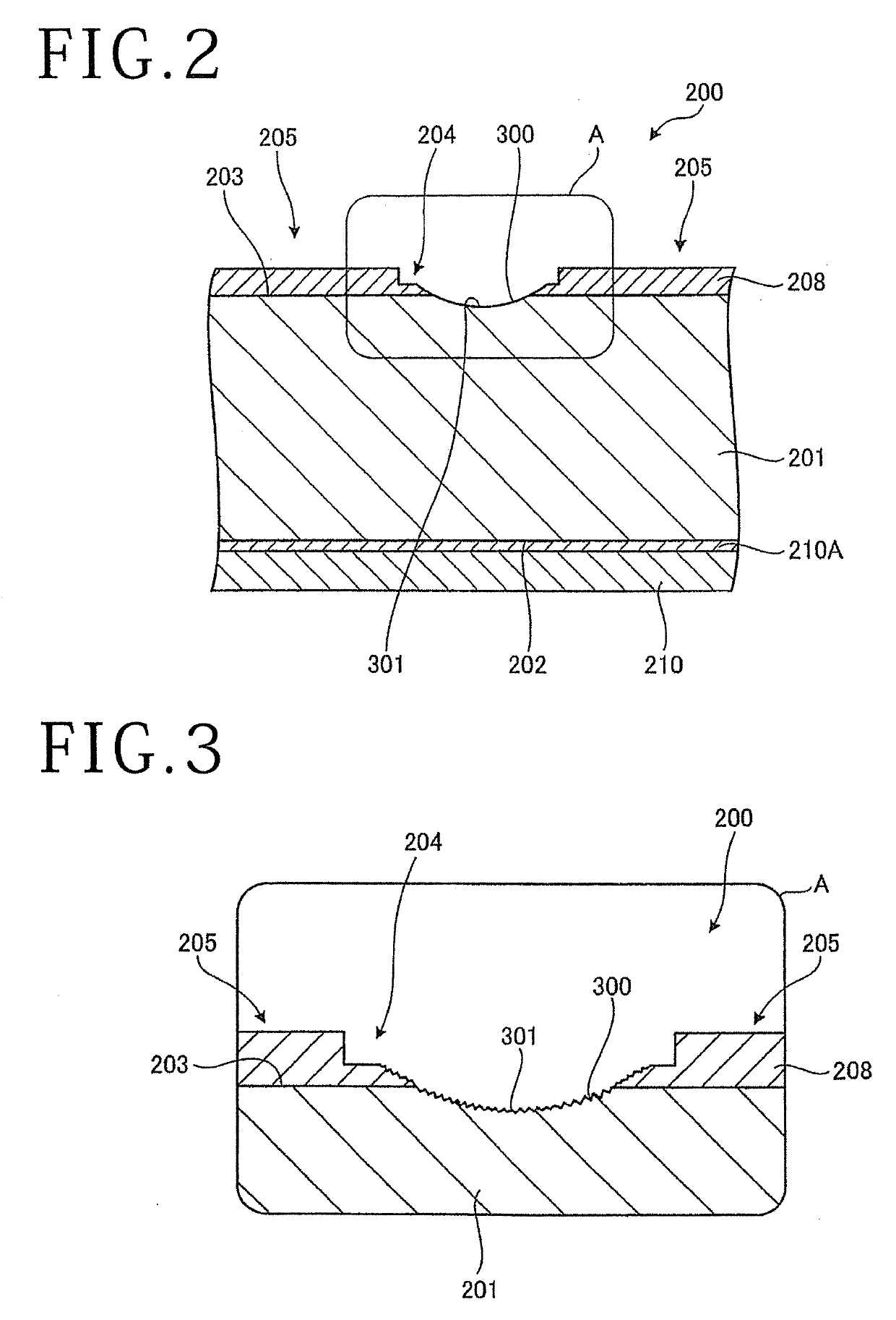
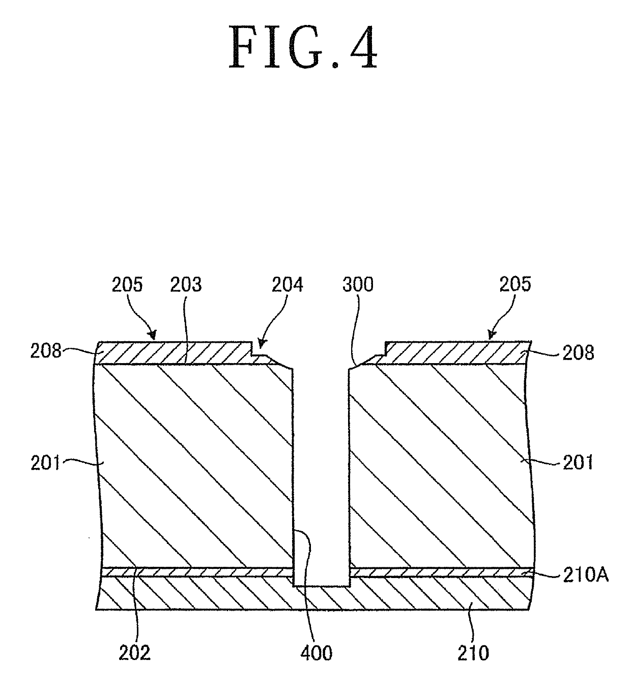
[0024]A cutting method of a workpiece according to the present embodiment of the present invention will be described based on the drawings. FIG. 1 is a perspective view of a workpiece that is a cutting target of the cutting method of a workpiece according to the present embodiment. FIG. 2 is a sectional view along line II-II in FIG. 1. FIG. 3 is an enlarged diagram of part A in FIG. 2. FIG. 4 is a sectional view of the workpiece in which a fully-cut groove is formed to overlap with a laser-processed groove. FIG. 5 is a perspective view illustrating a configuration example of a cutting apparatus used in the cutting method of a workpiece according to the present embodiment. FIG. 6 is a diagram illustrating a configuration of a photographic unit of the cutting apparatus illustrated in FIG. 5.
[0025]As illustrated in FIG. 1, a workpiece 200 according to the present embodiment is a circular-disc-shaped semiconductor wafer or optical device wafer including silicon, sapphire, gallium, or th...
PUM
 Abstract
Description
Claims
Application Information
 - R&D Engineer
- R&D Manager
- IP Professional
- Industry Leading Data Capabilities
- Powerful AI technology
- Patent DNA Extraction
Browse by: Latest US Patents, China's latest patents, Technical Efficacy Thesaurus, Application Domain, Technology Topic.
© 2024 PatSnap. All rights reserved.Legal|Privacy policy|Modern Slavery Act Transparency Statement|Sitemap