

Method of operating resistive memory device capable of reducing write latency
a resistive memory and write latency technology, applied in the direction of information storage, static storage, digital storage, etc., can solve the problem of long time taken to write or program data, and achieve the effect of reducing the write operation time of the data
- Summary
- Abstract
- Description
- Claims
- Application Information
AI Technical Summary
Benefits of technology
Problems solved by technology
Method used
Image

Examples
Embodiment Construction
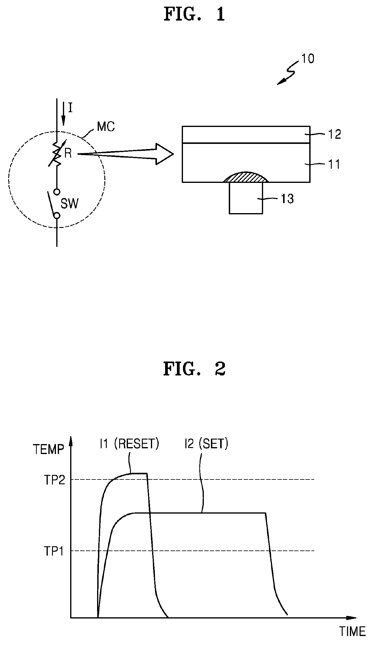
[0022]FIG. 1 is a schematic diagram of a memory cell MC using a method of operating a resistive memory device, according to an exemplary embodiment of the inventive concept.
[0023]Referring to FIG. 1, the memory cell MC includes a variable resistor R and a switch SW. The switch SW may be implemented using various devices such as a transistor and a diode. As magnified in FIG. 1, the variable resistor R may include a phase-change layer 11, an upper electrode 12 provided on the phase-change layer 11, and a lower electrode 13 provided under the phase-change layer 11. In an embodiment, the phase-change layer 11 is made of a germanium (Ge)-antimony (Sb)-tellurium (Te) (GST) material.
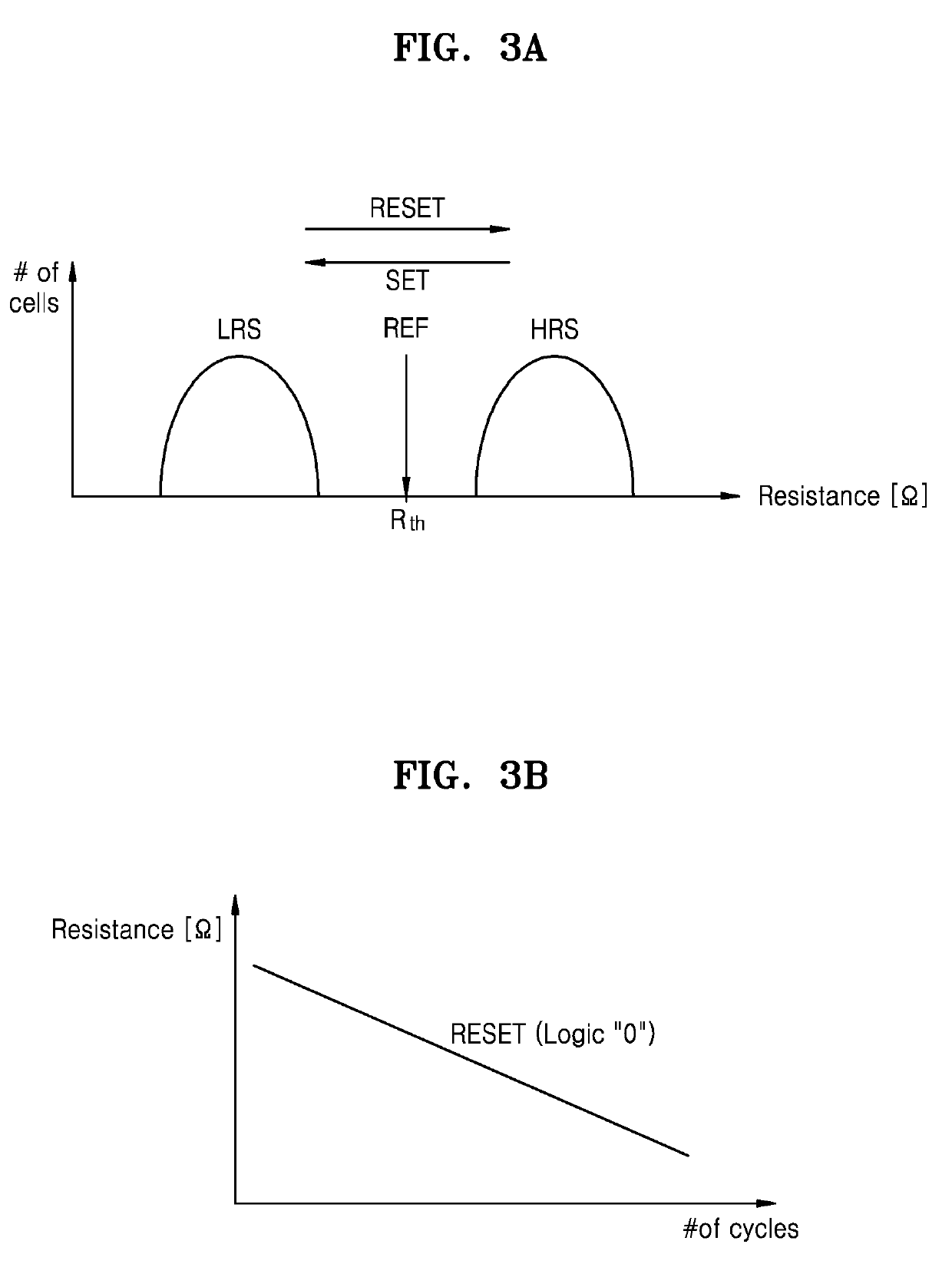
[0024]The GST material may be programmed between an amorphous state having high resistivity and a crystalline state having low resistivity. The GST material may be programmed by heating the GST material. A heating level and time may determine whether the GST material remains in an amorphous state or in a crysta...
PUM
 Abstract
Description
Claims
Application Information