
Semiconductor device and power converter

a technology of semiconductor devices and power converters, which is applied in semiconductor devices, solid-state devices, basic electric elements, etc., can solve the problems of resin flowability degradation in gaps, and achieve the effect of preventing the degradation of reliability and insulation properties and preventing the increase of manufacturing costs

Active Publication Date: 2019-09-26
MITSUBISHI ELECTRIC CORP
View PDF0 Cites 1 Cited by
  • Summary
  • Abstract
  • Description
  • Claims
  • Application Information

AI Technical Summary

Benefits of technology

The present invention relates to a semiconductor device with a conductive layer having a recess pattern to create a tunnel-like space that allows resin to flow through during a resin injection process. This prevents air bubbles from remaining inside the resin, which improves the reliability and insulation properties of the semiconductor device. Additionally, this simple configuration makes it easier to manufacture and reduces manufacture costs.

Problems solved by technology

This configuration, which creates a narrow gap between the adjacent semiconductor elements, degrades resin flowability in the gap when the inside of the semiconductor device is sealed with the resin.
The degraded resin flowability causes air to be trapped inside the resin in the gaps, thus remaining as air bubbles.

Method used


Image

  • Semiconductor device and power converter
  • Semiconductor device and power converter
  • Semiconductor device and power converter

Examples


first embodiment

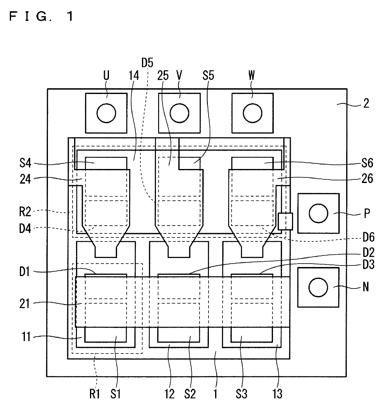
[0027]FIG. 1 is a plan view of a semiconductor device according to a first embodiment. The semiconductor device in the first embodiment is a three-phase (i.e., a U-phase, a V-phase, and a W-phase) semiconductor module used for, for instance, motor driving (that is, the semiconductor device includes six switching elements).

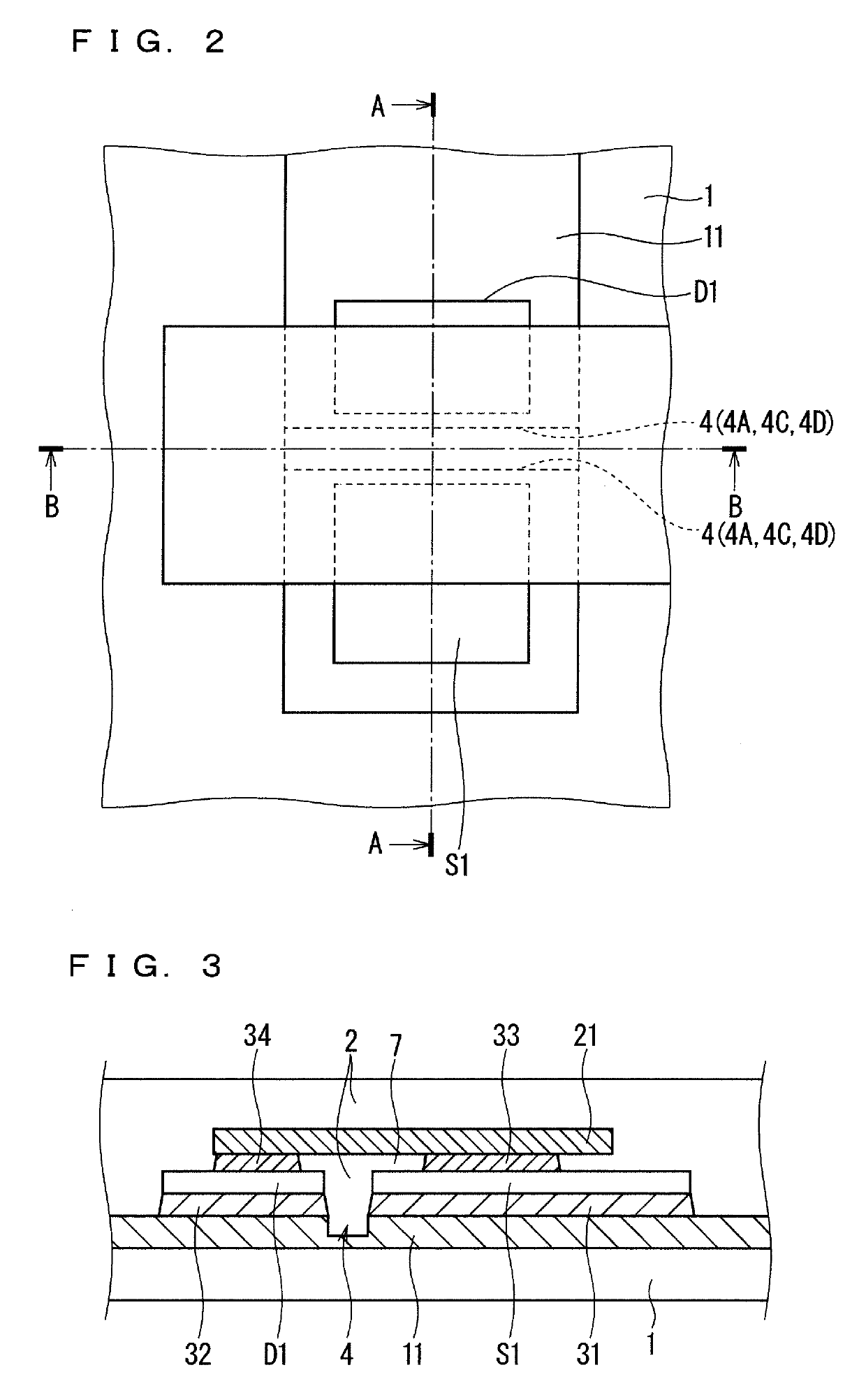
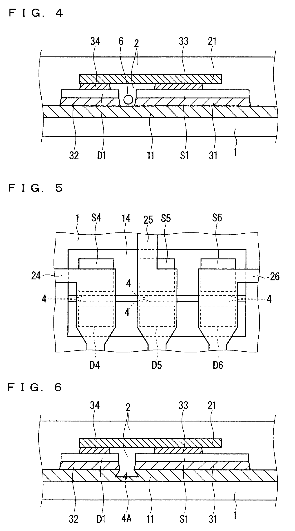
[0028]As illustrated in FIG. 1, the semiconductor device includes an insulating substrate 1, a plurality of conductive layers 11 to 14 disposed on the insulating substrate 1 so as to be separated from each other, six switching elements S1 to S6, six freewheeling diodes D1 to D6, and a plurality of electrodes 21 and 24 to 26. The conductive layers 11 to 14, the switching elements S1 to S6, and the freewheeling diodes D1 to D6 are sealed with resin 2. For easy illustration, FIG. 1 does not illustrate the resin 2 in the periphery of the conductive layers 11 to 14 in FIG. 1.

[0029]The conductive layers 11 to 14 are each made of, for instance, aluminum or an aluminum-con...

second embodiment

[0071]FIG. 10 is a plan view of a semiconductor device according to a second embodiment. The plan view in FIG. 10 corresponds to the enlarged plan view of the region R1 of the semiconductor device in FIG. 1. Further, FIG. 11 is a cross-sectional view of the semiconductor device taken along line C-C in FIG. 10.

[0072]The first embodiment has described that the recess pattern 4 of the semiconductor device is a groove. Meanwhile, the semiconductor device in the second embodiment has a recess pattern 5 provided with a plurality of recesses 51. The configuration of the semiconductor device in the second embodiment, which is the same as that of the semiconductor device in the first embodiment except the recess pattern 5, will be not elaborated upon.

[0073]As illustrated in FIG. 10, the recess pattern 5 is disposed on the upper surface of the conductive layer 11 (i.e., an opposite surface of the conductive layer 11 opposite from the insulating substrate 1). The recess pattern 5 is disposed a...

third embodiment

[0080]FIG. 12 is a cross-sectional view of a semiconductor device according to a third embodiment. The cross-section in FIG. 12 corresponds to the cross-section of the semiconductor device taken along line A-A in FIG. 2.

[0081]Like the corresponding one in the first embodiment, the recess pattern 4 in the third embodiment is disposed on the upper surface of the conductive layer 11 so as to extend along a gap between the switching element S1 and the freewheeling diode D1. Further, the electrode 21 in the third embodiment has a groove 211 disposed on a surface of the electrode 21 on a conductive-layer-11 side, so as to extend along the gap between the switching element S1 and the freewheeling diode D1 in plan view.

[0082]The semiconductor device in the third embodiment has the groove 211 on the electrode 21 in addition to a groove (i.e., the recess pattern 4) on the upper surface of the conductive layer 11. Accordingly, a tunnel-like portion is more enlarged that is defined by the condu...


PUM


Abstract

A semiconductor device according to the present invention includes the following: a conductive layer disposed on an insulating substrate; a first semiconductor element and a second semiconductor element that are joined on an opposite surface of the conductive layer opposite from the insulating substrate, with a gap the first semiconductor element and the second semiconductor element; an electrode joined on an opposite surface of the first semiconductor element opposite from the conductive layer, and an opposite surface of the second semiconductor element opposite from the conductive layer, so as to extend over the gap; and resin sealing the conductive layer, the first semiconductor element, the second semiconductor element, and the electrode. The conductive layer has a recess pattern that is disposed on a surface being opposite from the insulating substrate and facing the gap, the recess pattern extending along the gap.

Description

TECHNICAL FIELD[0001]The present invention relates to a semiconductor device and a power converter.BACKGROUND ART[0002]Semiconductor devices having a plurality of semiconductor elements (e.g., switching elements) are used in apparatuses, such as inverters that control the motors of, for instance, electric vehicles or trains, and converters for energy regeneration. The inside of such a semiconductor device is typically sealed with resin.[0003]The semiconductor device is configured in such a manner that the semiconductor elements are arranged to be adjacent to each other on a conductive layer, and that an electrode is joined in common on the upper surfaces of the adjacent semiconductor elements (c.f., Patent Document 1).[0004]This configuration, which creates a narrow gap between the adjacent semiconductor elements, degrades resin flowability in the gap when the inside of the semiconductor device is sealed with the resin. The degraded resin flowability causes air to be trapped inside ...

Claims


Application Information

Patent Timeline
Patent Type & Authority Applications(United States)
IPC IPC(8): H01L23/31H02M7/5387H01L25/07
CPCH01L25/072H01L23/3121H02M7/53875H01L23/12H01L25/18H01L2224/40137H01L2224/33181H01L23/4824H02M7/5387H02M7/003H01L2224/32225H01L2224/26175H01L25/07
Inventor TANAKA, MITSUGUISHIYAMA, YUSUKESHIRAO, AKITOSHI
Owner MITSUBISHI ELECTRIC CORP
Learn More