Method of manufacturing light emitting diode package

Inactive Publication Date: 2007-07-05
SAMSUNG ELECTRONICS CO LTD
View PDF10 Cites 17 Cited by
  • Summary
  • Abstract
  • Description
  • Claims
  • Application Information

AI Technical Summary

Benefits of technology

[0013] The present invention has been made to solve the foregoing problems of the prior art and therefore an aspect of the present invention is to provide a method of manufacturing an LED package in which a resilient resin is dispensed on an LED package body and an entire structure is overturned by

Problems solved by technology

However, the conventional method of manufacturing the LED package has following drawbacks.
First, the LED lens 40 is separately prepared using the mold 36 for fabrication of lens, incurring extra proce

Method used


Image

  • Method of manufacturing light emitting diode package
  • Method of manufacturing light emitting diode package
  • Method of manufacturing light emitting diode package

Examples


Embodiment Construction

[0026] Exemplary embodiments of the present invention will now be described in detail with reference to the accompanying drawings.

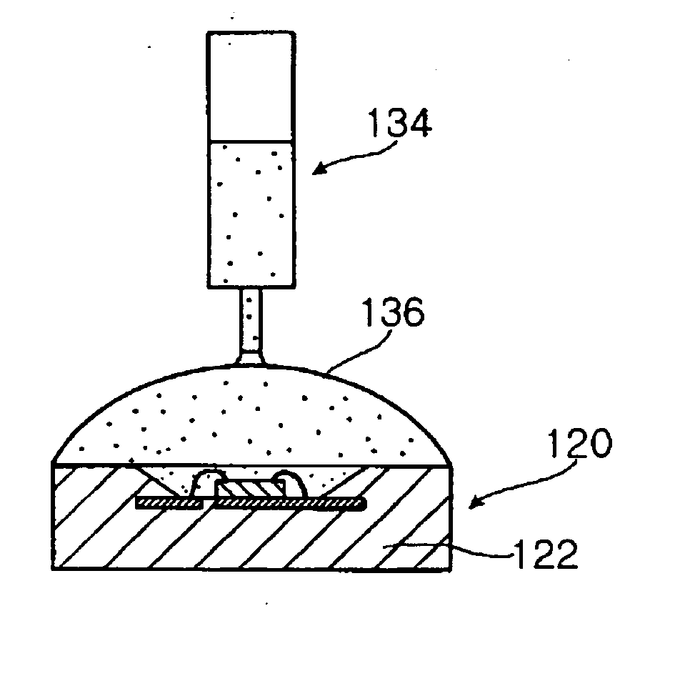
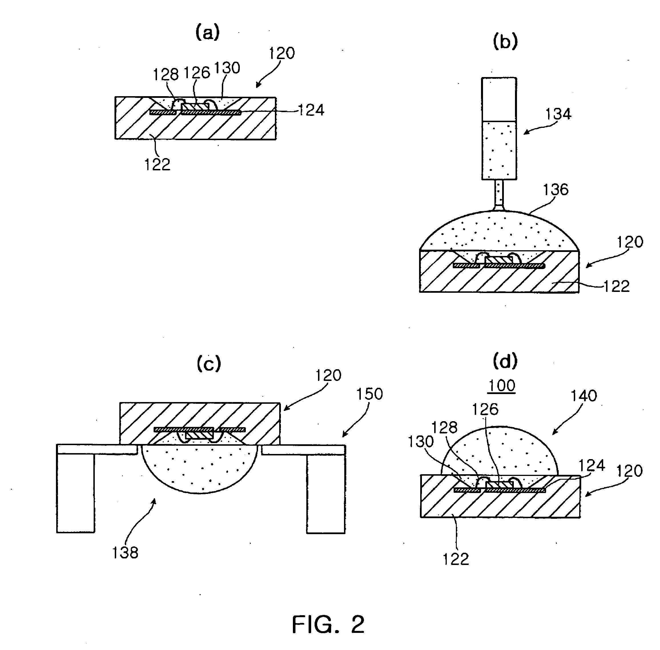
[0027]FIG. 2 is a schematic view illustrating a manufacturing process of an LED package according to the present invention.

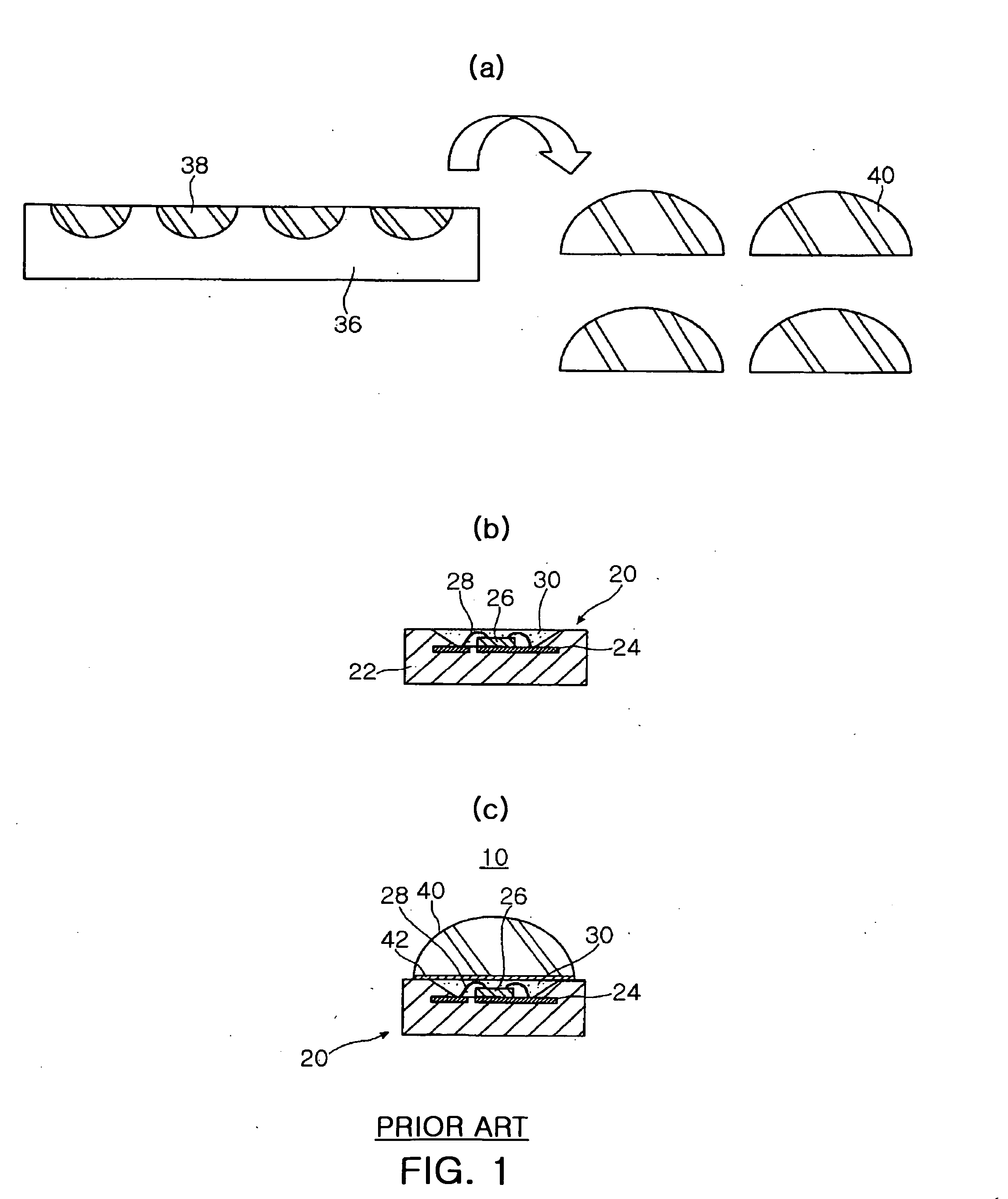
[0028] First, FIG. 2(a) illustrates a step of forming the LED package body of the LED package according to the present invention. To form the LED package body 120, a pair of leads 124 are formed on a substrate or a substrate part 122 having a recess formed in an upper surface thereof, an LED chip 126 is mounted on the lead 124 and electrically connected to the lead 124 by wires 128, and a resilient resin such as transparent silicone is filled in the recess to form a transparent encapsulant 130. Here, the LED chip 126 can also be connected to the lead 124 by a solder bump (not shown) instead of the wires 128.

[0029] In this case, a transparent resilient resin is used for the resilient encapsulant 130 instead of a general transparent ...


PUM

PropertyMeasurementUnit
Temperatureaaaaaaaaaa
Massaaaaaaaaaa
Massaaaaaaaaaa

Abstract

A method of manufacturing an LED package. The method includes dispensing a transparent resilient resin on an LED package body and overturning an entire structure to form an LED lens integrally provided to the LED package body. This prevents extra processes and costs incurring from forming intermediate layers and obviates degradation in reliability and light extraction efficiency due to additional interfaces.

Description

CLAIM OF PRIORITY [0001] This application claims the benefit of Korean Patent Application No. 2006-0001519 filed on Jan. 5, 2006, in the Korean Intellectual Property Office, the disclosure of which is incorporated herein by reference. BACKGROUND OF THE INVENTION [0002] 1. Field of the Invention [0003] The present invention relates to a Light Emitting Diode (LED) package and, more particularly, to a method of manufacturing an LED package in which a transparent resilient resin is dispensed on an LED package body and an entire structure is overturned by an overturning technique to form an LED lens integrally with the LED package body, preventing extra processes and costs incurred from forming intermediate layers, thereby obviating degradation in reliability and light extraction efficiency. [0004] 2. Description of the Related Art [0005] In general, a Light Emitting Diode (LED) is a semiconductor device for generating light of various colors in response to application of current. The co...

Claims


Application Information

Patent Timeline
IPC IPC(8): H01L21/00H01L33/54H01L33/56H01L33/60H01L33/62
CPCB29C41/12B29C41/20B29C41/36B29C41/50B29L2011/00H01L2224/48091H01L33/52H01L2924/00014B29D11/00019B29D11/00365B29D11/00432F02B51/04F02M27/045
Inventor KIM, YONG SIKCHOI, SEOG MOONKIM, YONG SUKSHIN, SANG HYUN
Owner SAMSUNG ELECTRONICS CO LTD
Why Eureka
Try Eureka