Method Of Manufacturing Sealed Electronic Component And Sealed Electronic Component
- Summary
- Abstract
- Description
- Claims
- Application Information
AI Technical Summary
Benefits of technology
Problems solved by technology
Method used
Image
Examples
first embodiment
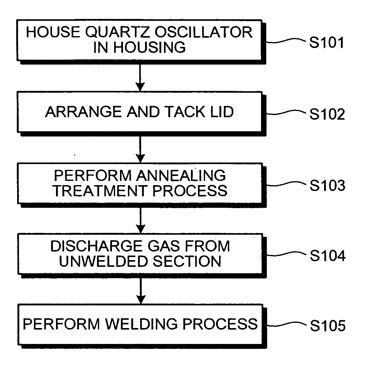
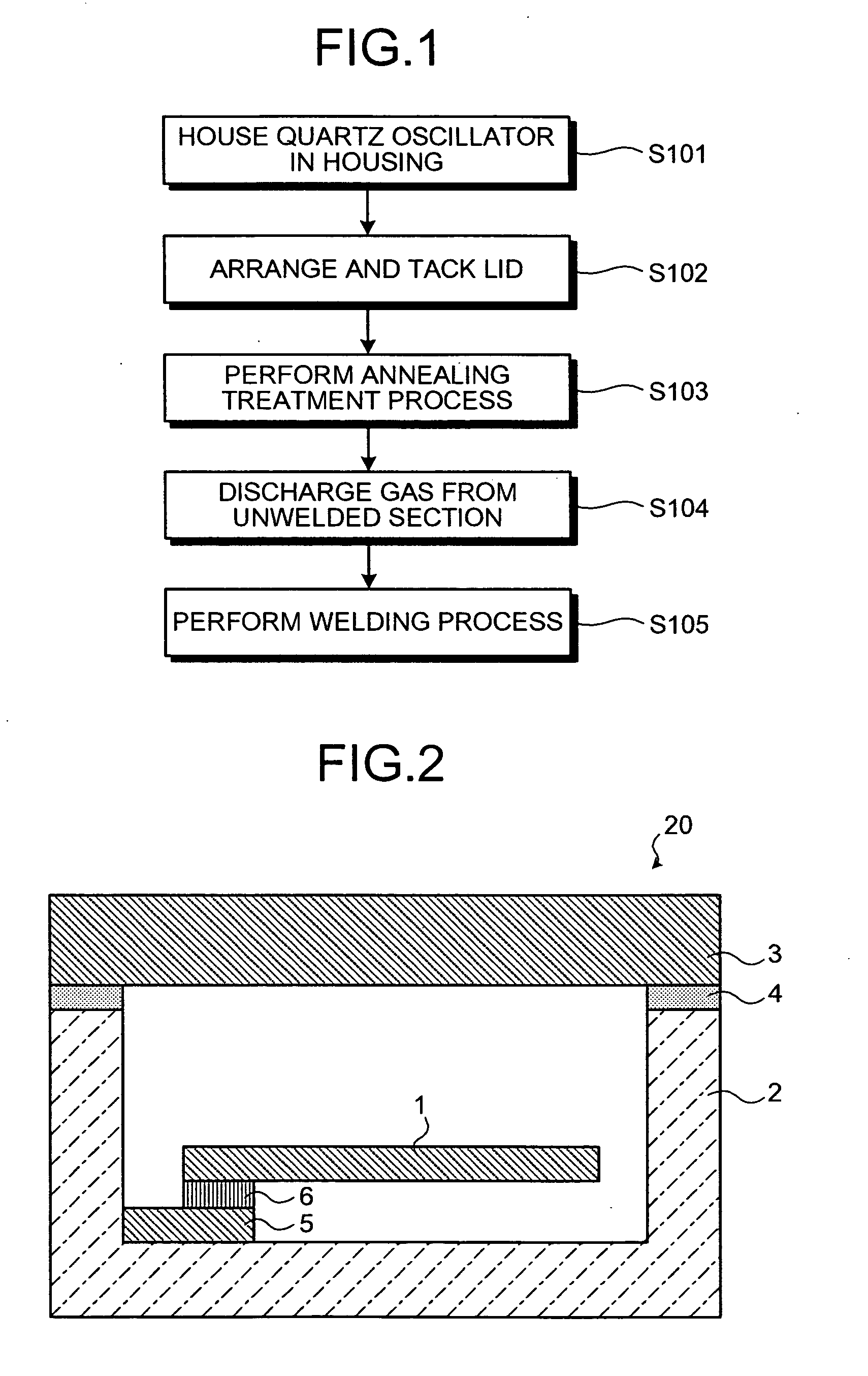
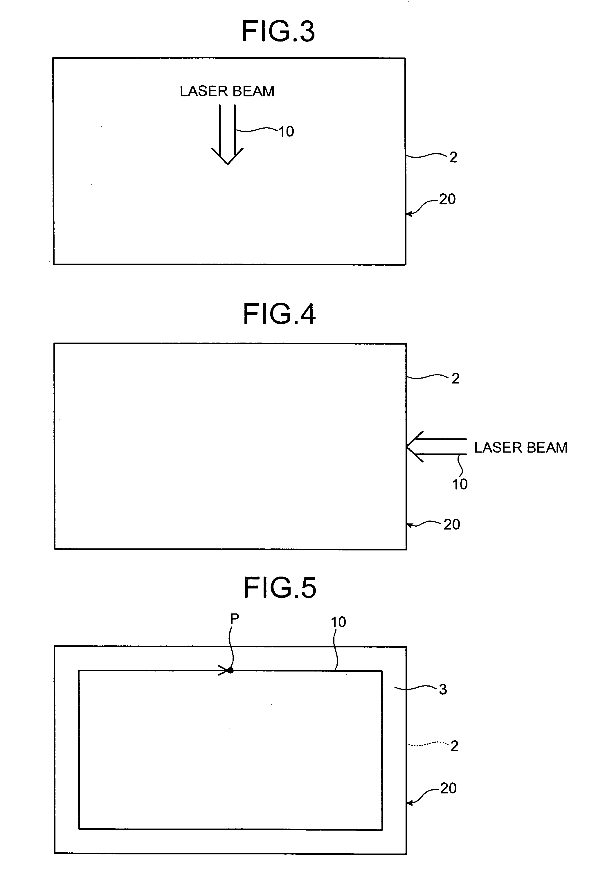
[0088]FIG. 1 is a flow chart illustrating respective processes in the manufacturing method of a package according to a first embodiment of the present invention. FIG. 2 is a schematic cross sectional view of the package manufactured by the manufacturing method of FIG. 1. FIGS. 3 through 5 are schematic plan views for explaining the respective processes in the manufacturing method of FIG. 1. Specifically, FIGS. 3 and 4 illustrate a laser irradiation method in an annealing process of FIG. 1, while FIG. 5 illustrates a locus of the laser in a welding process of FIG. 1. While an electron beam, an ion beam, the laser (a solid state laser, a gas laser, and a semiconductor laser), and a microwave may be used as a beam, the electron beam and the semiconductor laser are particularly easy to use. In the present embodiment, there will be described the case where the laser is used.
[0089] As shown in FIG. 1, in the manufacturing method of the package of the present embodiment, a quartz oscillat...
second embodiment
[0110]FIGS. 6 through 9 are figures for explaining the manufacturing method of the package according to a second embodiment of the present invention. Specifically, FIG. 6 is a plan view of the housing used for the package of the present embodiment seen from the bottom, while FIGS. 7 through 9 are schematic cross sectional views illustrating the welding process of the manufacturing method according to the present embodiment.
[0111] Although the manufacturing method of the package according to the present embodiment includes the respective process steps S101 through S105 illustrated in the flowchart of FIG. 1, as with the case of the first embodiment, to manufacture the package 20 of FIG. 2, the followings are different from the first embodiment.
[0112] As shown in FIG. 6, in the package 20 of the present embodiment, the bottom of the housing 2 is provided with a through hole 500 to cause the interior of the package 20 (i.e., the housing portion of the housing 2 for the quartz oscilla...
third embodiment
[0124]FIG. 10 is a flowchart illustrating the respective processes in the manufacturing method of the package according to a third embodiment of the present invention. FIGS. 11 through 14 are schematic plan views for explaining the electron beam irradiation method in the respective processes of the manufacturing method of FIG. 10, illustrating the locus of the electron beam irradiated to the package from the lid side. Specifically, FIGS. 11 and 12 illustrate the locus of the electron beam in a primary welding process at step S203 of FIG. 10, FIG. 13 illustrates the locus of the electron beam in an annealing process at step S204 of FIG. 10, and FIG. 14 illustrates the locus of the electron beam in a secondary welding process at step S206 of FIG. 10.
[0125] In the package manufacturing method of the present embodiment, as shown in FIG. 10, the quartz oscillator 1 is firstly housed in the housing 2 of FIG. 2 (step S201). Then, by the method described above in step S102 of FIG. 1 of the...
PUM
| Property | Measurement | Unit |
|---|---|---|
| Electrical resistance | aaaaa | aaaaa |
| Electrical resistance | aaaaa | aaaaa |
| Temperature | aaaaa | aaaaa |
Abstract
Description
Claims
Application Information


