Supercharge Your Innovation With Domain-Expert AI Agents!

Vertical Transistors with Different Gate Lengths

a technology of vertical transistors and gate lengths, applied in the direction of semiconductor devices, semiconductor/solid-state device details, electrical apparatus, etc., can solve the problem of difficulty in implementing fets of different lengths in vfet architectur

Active Publication Date: 2020-02-06
INT BUSINESS MASCH CORP
View PDF8 Cites 0 Cited by
  • Summary
  • Abstract
  • Description
  • Claims
  • Application Information

AI Technical Summary

Benefits of technology

Enables the effective formation of VFETs with differing gate lengths, reducing power consumption by leveraging 'wimpy' transistors along non-critical paths, while maintaining the same physical gate length for both types of VFETs, thus improving chip efficiency.

Problems solved by technology

However, it is difficult to implement FETs of differing lengths in VFET architecture due to challenges in aligning the junction with the physical gate.

Method used


Image

  • Vertical Transistors with Different Gate Lengths
  • Vertical Transistors with Different Gate Lengths
  • Vertical Transistors with Different Gate Lengths

Examples


Embodiment Construction

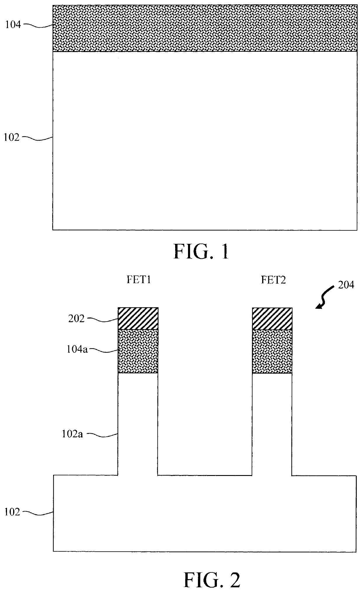
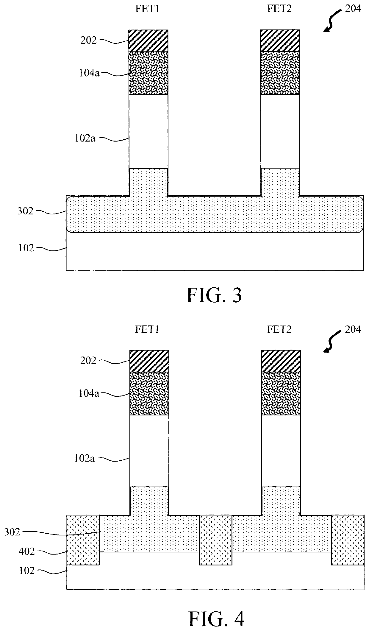
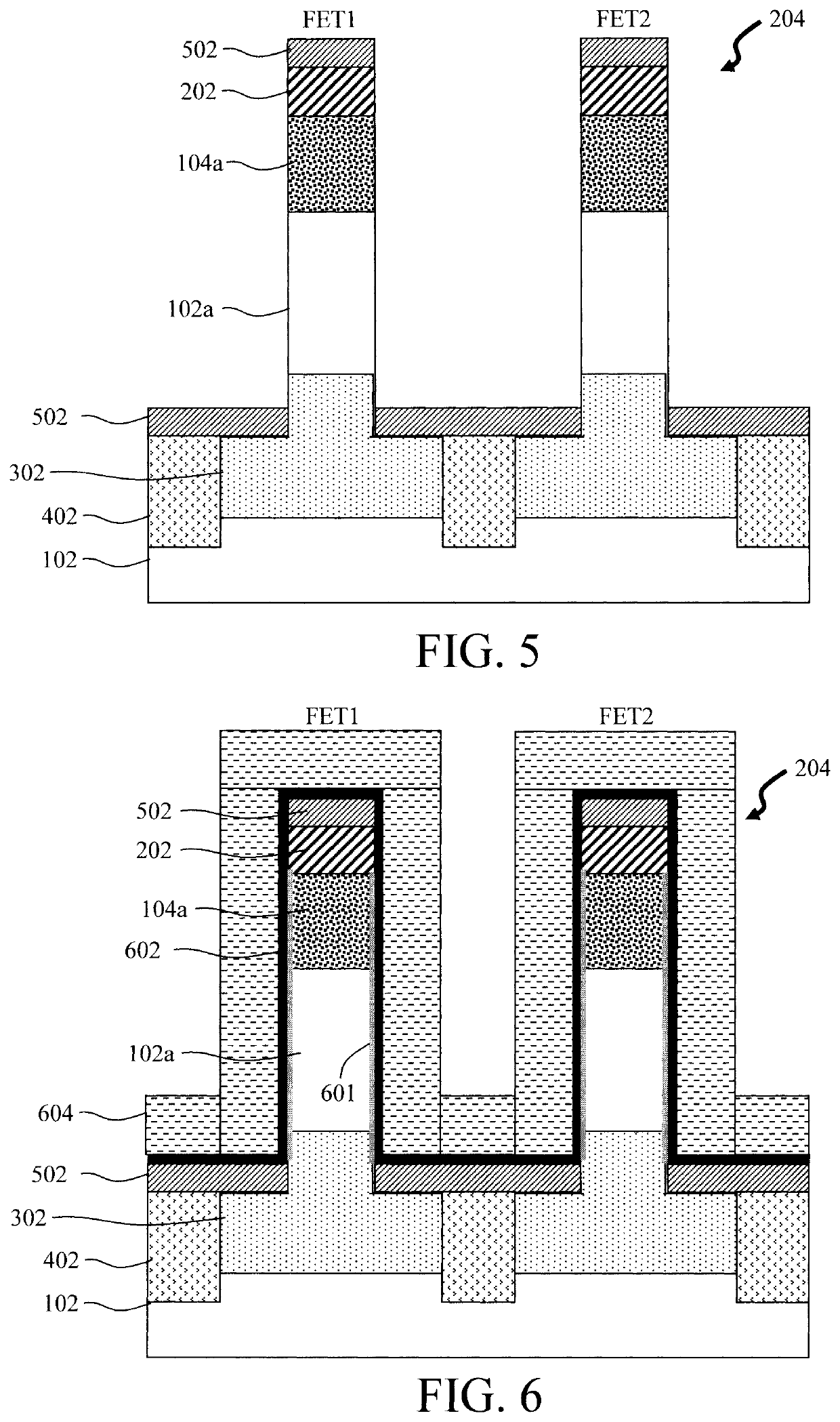
[0038]Provided herein are techniques for effectively forming vertical field effect transistors (VFETs) with differing effective gate lengths (Lgate) on the same chip. Reference is made herein to ‘Wimpy’ VFETs, which are VFETs with an Lgate that is slightly greater than a nominal VFET transistor. For instance, the Lgate of a wimpy VFET is from about 1.5 nanometers (nm) to about 10 nm and ranges therebetween greater than the Lgate of a nominal VFET. As provided above, employing these ‘wimpy’ transistors along non-critical paths in the chip circuitry can reduce power consumption. Advantageously, the present techniques can be leveraged to form both types of VFET devices (i.e., wimpy and nominal VFETs) on the same chip.

[0039]In the description that follows reference will be made to two VFET designs, one having a longer gate length Lgate1, and another having a regular gate length Lgate2, i.e., Lgate1>Lgate2. As provided above, the difference between Lgate1 and Lgate2, i.e., Lgate1-Lgate2,...


PUM


Abstract

Techniques for forming VFETs with differing gate lengths are provided. In one aspect, a method for forming a VFET device includes: patterning fins in a substrate, wherein at least one of the fins includes a vertical fin channel of a FET1 and at least another one of the fins includes a vertical fin channel of a FET2; forming a bottom source and drain; forming bottom spacers on the bottom source and drain; forming gates surrounding the vertical fin channel of the FET1 and FET2; forming top spacers on the gate; and forming top source and drains at the tops of the fins by varying a positioning of the top source and drains relative to at least one of the vertical fin channel of the FET1 and the FET2 such that the FET1 / FET2 have an effective gate length Lgate1 / Lgate2, wherein Lgate1>Lgate2. A VFET device is also provided.

Description

CROSS-REFERENCE TO RELATED APPLICATIONS[0001]This application is a divisional of U.S. application Ser. No. 15 / 812,843 filed on Nov. 14, 2017, the contents of which are incorporated by reference herein.FIELD OF THE INVENTION[0002]The present invention relates to vertical field effect transistors (VFETs), and more particularly, to techniques for forming VFETs with differing gate lengths on the same chip.BACKGROUND OF THE INVENTION[0003]As opposed to planar complementary metal-oxide-semiconductor (CMOS) devices, vertical field effect transistors (VFETs) are oriented with a vertical fin channel disposed on a bottom source / drain and a top source / drain disposed on the fin channel. VFETs have been pursued as a potential device option for scaling CMOS to the 5 nanometer (nm) node and beyond.[0004]A reduction in chip power consumption can be realized by increasing the gate length (Lgate) of transistors (as compared to nominal transistors) along non-critical paths on the chip as this reduces ...

Claims


Application Information

Patent Timeline
Patent Type & Authority Applications(United States)
IPC IPC(8): H01L27/088H01L21/8234H01L23/522H01L29/78H01L29/66H01L29/08H01L29/786
CPCH01L23/5226H01L21/823418H01L29/66666H01L29/165H01L29/7827H01L21/823475H01L29/0847H01L27/088H01L21/823456H01L21/823487H01L29/78642H01L29/41741H01L29/42376
Inventor MIAO, XINZHANG, CHENCHENG, KANGGUOLI, JUNTAO
Owner INT BUSINESS MASCH CORP
Features
  • R&D
  • Intellectual Property
  • Life Sciences
  • Materials
  • Tech Scout
  • Unparalleled Data Quality
  • Higher Quality Content
  • 60% Fewer Hallucinations
Learn More