Pixel arrangement structure, display substrate, display apparatus and method of fabrication thereof

a technology of pixel arrangement and display substrate, which is applied in the field of display technology, can solve the problems of increasing the difficulty of manufacturing and cost of the display device, the difficulty of producing a high ppi (pixel density) display device, and the difficulty of the present fmm process to achieve the desired pixel density

Active Publication Date: 2020-02-06
CHENGDU BOE OPTOELECTRONICS TECH CO LTD +1
View PDF0 Cites 16 Cited by
  • Summary
  • Abstract
  • Description
  • Claims
  • Application Information

AI Technical Summary

Benefits of technology

[0038]An example of the present disclosure is a pixel arrangement structure, comprising a plurality of repeating units, wherein each of the plurality of repeating units comprises two first sub-pixels, one second sub-pixel, and one third sub-pixel; in each of the plurality of repeating units, the two first sub-pixels form a first sub-pixel pair; the one second sub-pixel, the first sub-pixel pair, and the one third sub-pixel are arranged in a first direction; and the two first sub-pixels in the first sub-pixel pair are arranged in a second direction intersecting the first direction; the plurality of repeating units are arranged in the first direction to form a plurality of repeating unit groups, and the plurality of repeating unit groups are arranged in the second direction; the repeating units in adjacent ones of the plurality of repeating unit groups are misaligned with each other in the second direction, and the repeating units in two repeating unit groups which are separated from each other by one repeating unit group a

Problems solved by technology

The requirement that display devices have high display resolution increases the difficulty of manufacturing and cost of the display device.
In particular, in the present AMOLED (Active Matrix Organic Light-Emitting Diode) field, due to the limitations of the

Method used


Image

  • Pixel arrangement structure, display substrate, display apparatus and method of fabrication thereof
  • Pixel arrangement structure, display substrate, display apparatus and method of fabrication thereof
  • Pixel arrangement structure, display substrate, display apparatus and method of fabrication thereof

Examples


Embodiment Construction

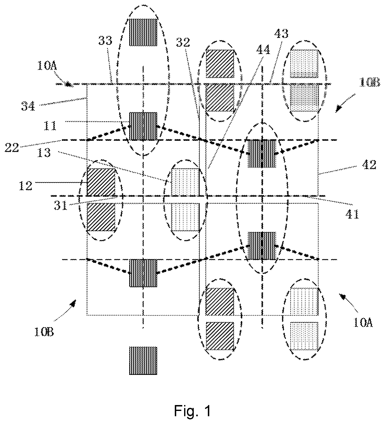
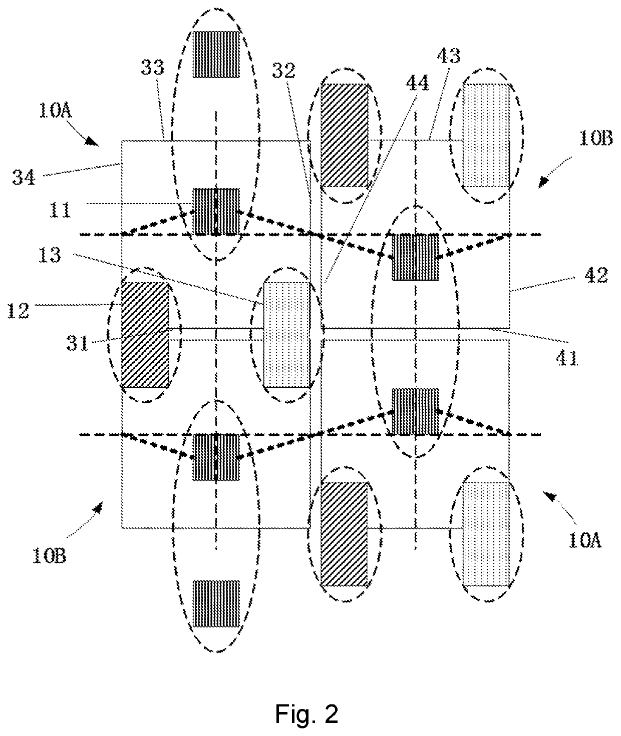
[0054]The present disclosure is described with reference to embodiments of the invention. Throughout the description of the invention reference, is made to FIGS. 1-3. When referring to the figures, like structures and elements shown throughout are indicated with like reference numerals.

[0055]Unless otherwise defined, technical terms or scientific terms used herein should be in the ordinary meaning as understood by those of ordinary skill in the art to which this invention belongs. The terms “first,”“second,” and the like as used in the specification and claims are not intended to imply any order, quantity or importance, but only to distinguish between the different components. Likewise, the terms “a” and the like do not denote a numerical limitation, but rather denote the presence of at least one. The terms “connected” and the like are not limited to physical or mechanical connections, regardless of whether it is direct or indirect. The terms “upper,”“lower,”“left,”“right” and the l...


PUM


Abstract

A pixel arrangement structure are provided, which includes a plurality of repeating units. Each of the plurality of repeating units includes two first sub-pixels, one second sub-pixel, and one third sub-pixel. Each of the first sub-pixel, the second sub-pixel and the third sub-pixel includes a pixel defining layer, the pixel defining layer includes a pixel defining layer opening to define an effective light emitting region of each sub-pixel; a plurality of first sub-pixels are arranged along the second direction to form a plurality of first sub-pixel groups, orthographic projections of pixel defining layer openings of the first sub-pixels in adjacent ones of the plurality of first sub-pixel groups on a straight line parallel to the second direction do not overlap each other.

Description

CROSS-REFERENCE TO RELATED APPLICATIONS[0001]This application is a continuation in part of U.S. Ser. No. 15 / 578,481 filed on Nov. 30, 2017 which is a national stage application of international application PCT / CN2017 / 075957 filed on Mar. 8, 2017, which claims priority from CN201610585894.4 filed on Jul. 22, 2016.[0002]This application is a continuation in part application of PCT / CN2019 / 098707 filed on Jul. 31, 2019. This application is also a continuation in part of PCT / CN2019 / 098705 filed on Jul. 31, 2019.[0003]This application is also a continuation in part application of PCT / CN2019 / 086875 filed on May 14, 2019, which claims priority from U.S. Ser. No. 16 / 234,777 filed on Dec. 28, 2018 (hereinafter the 777 application) which is a continuation in part of U.S. Ser. No. 15 / 536,347 filed on Jun. 15, 2017, now issued as Ser. No. 10,274,654, on Apr. 30, 2019 which is a national stage application of international application PCT / CN2016 / 081097 filed on May 5, 2016, which claims priority f...

Claims


Application Information

Patent Timeline
IPC IPC(8): H01L27/32G09G3/3225G09G3/3233H01L51/52
CPCG09G3/3233G09G2300/0452H01L27/3279G09G2300/0842G09G2310/0251H01L27/3218H01L27/3276H01L27/3216H01L51/525G09G2310/0262G09G3/3225H01L27/3246G09G2300/0426G09G2300/0814G09G2300/0819H10K59/352H10K59/353H10K59/123H10K59/131H10K50/8428H10K59/122H10K59/1315
Inventor HUANGFU, LUJIANGLIU, LIBINJI, FENGLIJIN, XIAODANLIANG, YINANLI, MEIZHANG, JIELUO, CHANGWU, JIANPENGWANG, HONGLI
Owner CHENGDU BOE OPTOELECTRONICS TECH CO LTD
Why Eureka
Try Eureka