
Display apparatus and manufacturing method thereof

a technology of display apparatus and manufacturing method, applied in the direction of electrical apparatus, basic electric elements, semiconductor devices, etc., can solve the problems of low production yield rate, high price, and oled panel, and achieve the effect of improving flatness

Active Publication Date: 2020-02-20
SAMSUNG ELECTRONICS CO LTD
View PDF3 Cites 8 Cited by
  • Summary
  • Abstract
  • Description
  • Claims
  • Application Information

AI Technical Summary

Benefits of technology

The present disclosure provides an encapsulation technology that can protect inorganic light emitting diodes from being physically damaged during transfer from a wafer to a substrate. Additionally, this technology can improve image quality and prevent seam between adjacent units in a matrix display. Furthermore, the patent enables easy repair of defective inorganic light emitting diodes after encapsulation.

Problems solved by technology

However, the OLED panel has some limitations such as the high price caused by a low production yield rate, the low reliability with a large size panel, and the durability that is affected by external surrounding such as water.
The inorganic light emitting display technology has its own challenges in transferring an inorganic light emitting diode in a very small size (having a size of several micrometers to several hundreds of micrometers) from a wafer to a substrate.
In addition, even after the inorganic light emitting diode is mounted, there are still challenges in physically protecting the inorganic light emitting diode without affecting the display with the optical distortion and the optical loss.

Method used


Image

  • Display apparatus and manufacturing method thereof
  • Display apparatus and manufacturing method thereof
  • Display apparatus and manufacturing method thereof

Examples


Embodiment Construction

[0051]Embodiments described in the disclosure and configurations shown in the drawings are merely examples of the disclosure, and may be modified in various different ways at the time of filing of the present application to replace the embodiments and drawings of the disclosure.

[0052]The singular forms “a,”“an” and “the” are intended to include the plural forms as well, unless the context clearly indicates otherwise. The shape and size of the elements in the figures may be exaggerated for clarity.

[0053]In this disclosure, the terms “including”, “having”, and the like are used to specify features, numbers, steps, operations, elements, components, or combinations thereof, but do not preclude the presence or addition of one or more of the features, elements, steps, operations, elements, components, or combinations thereof.

[0054]The present disclosure will be described more fully hereinafter with reference to the accompanying drawings

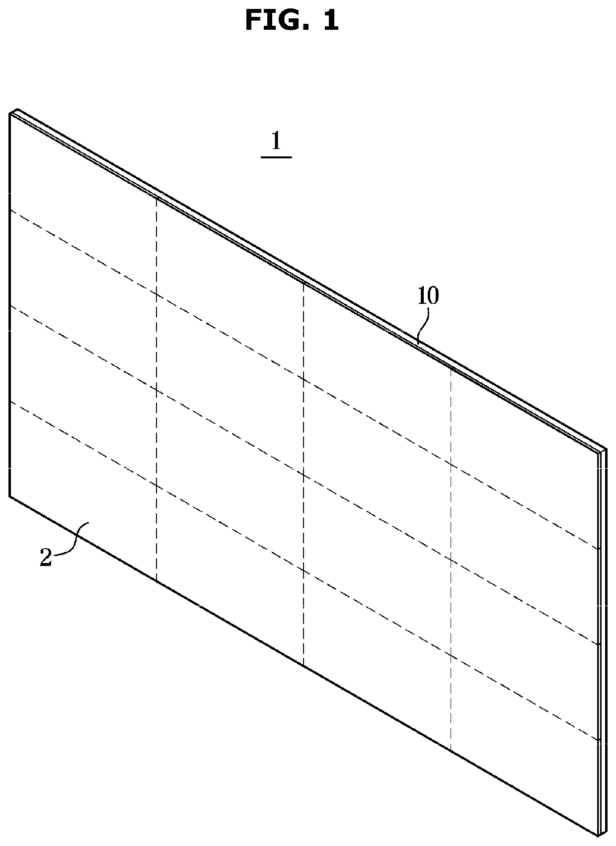
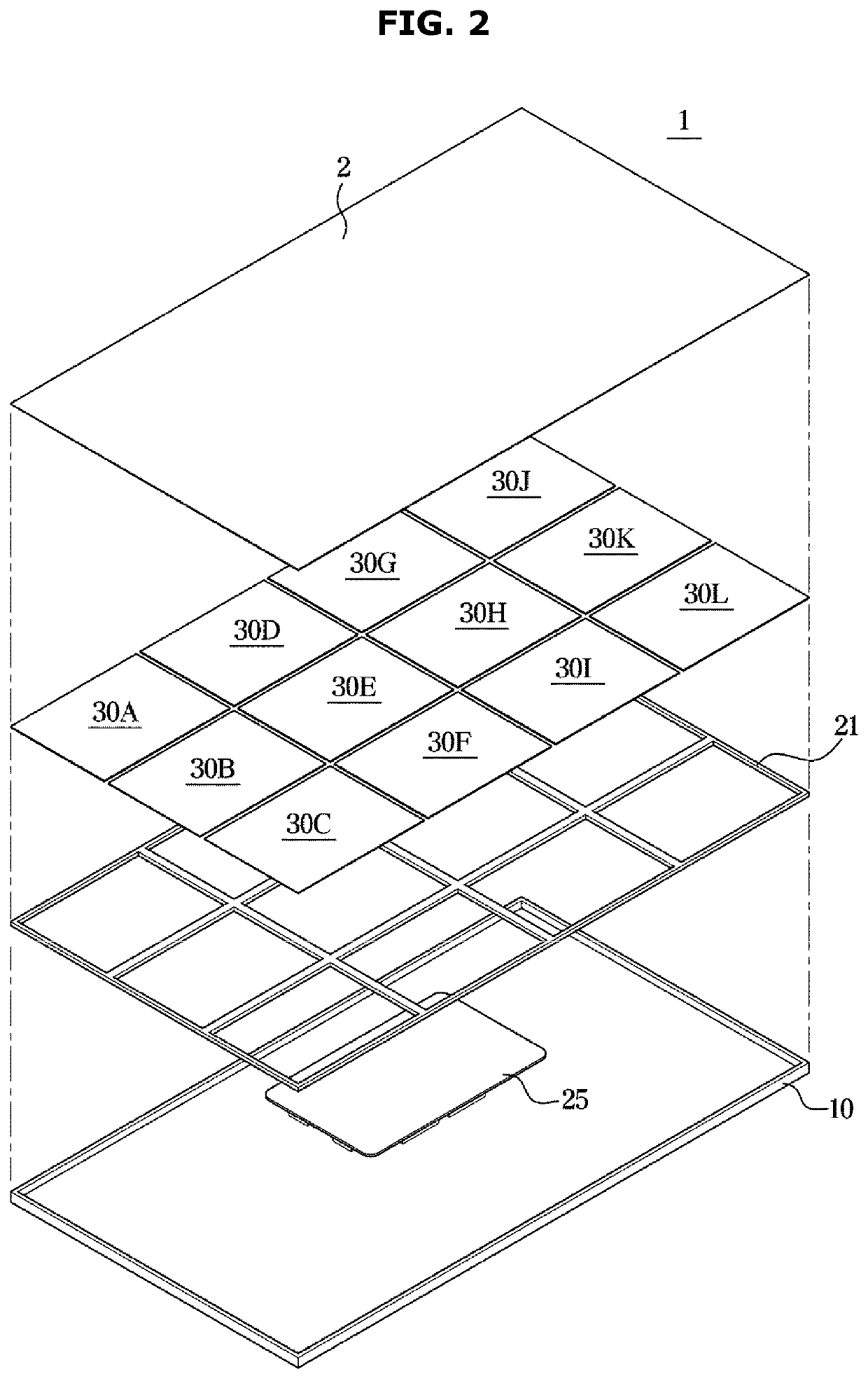
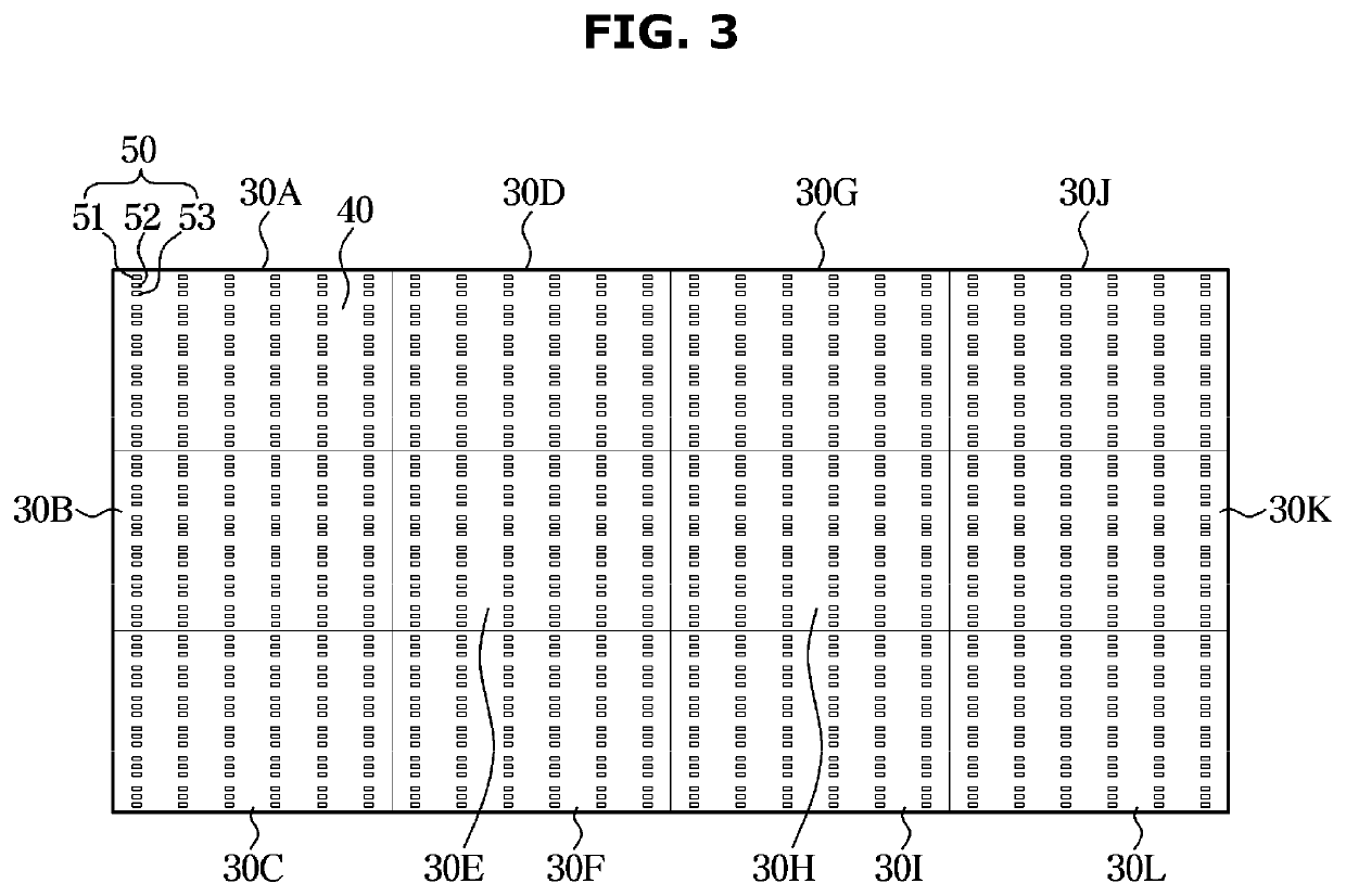
[0055]FIG. 1 is a perspective view of a display appar...


PUM

PropertyMeasurementUnit
sizeaaaaaaaaaa
temperatureaaaaaaaaaa

Abstract

A display apparatus includes a plurality of unit modules; and a cover configured to support the plurality of unit modules. Each of the plurality of unit modules includes: a substrate; a plurality of inorganic light emitting diodes provided on a mounting surface of the substrate; and an encapsulation layer formed on the mounting surface of the substrate to cover the plurality of inorganic light emitting diodes and the mounting surface of the substrate. The encapsulation layer includes a viscoelastic material having varying viscoelasticity based on temperature being applied to the viscoelastic material.

Description

CROSS-REFERENCE TO RELATED APPLICATIONS[0001]This application is based on and claims priority under 35 U.S.C. § 119 to Korean Patent Application No. 10-2018-0097032 filed on Aug. 20, 2018, and Korean Patent Application No. 10-2019-0089452 filed on Jul. 24, 2019, in the Korean Intellectual Property Office, the disclosures of which are incorporated by reference herein in their entireties.BACKGROUND1. Field[0002]The disclosure relates to a display apparatus capable of directly displaying an image by coupling a plurality of modules, each of the plurality of modules including a self-emissive inorganic light emitting diode is mounted on a substrate, to one another and a method of manufacturing the same.2. Description of Related Art[0003]A display apparatus is a type of an output device which visually displays information such as characters and figures, and images. The demand for high luminance, high resolution, large size, high efficiency, and low power display apparatuses is continuously...

Claims


Application Information

Patent Timeline
Patent Type & Authority Applications(United States)
IPC IPC(8): H01L33/54H01L27/15H01L33/56H01L27/12
CPCH01L27/156H01L33/56H01L33/54H01L27/1218H01L25/0753H01L33/62
Inventor PARK, WON SOONLEE, TACK MOYOON, JUNG HOON
Owner SAMSUNG ELECTRONICS CO LTD
Learn More