This helps you quickly interpret patents by identifying the three key elements:
Problems solved by technology
Method used
Benefits of technology
Benefits of technology
The present disclosure has various advantages and benefits. This patent is just a brief description of some of the technical effects. More information can be found by reading the patent itself.
Problems solved by technology
However, in such a light emitting display device, some light of light emitted from a light emitting layer is not externally discharged due to total reflection or the like at an interface between the light emitting layer and an electrode and / or an interface between the substrate and an air layer and thus light extraction efficiency decreases.
Accordingly, a light emitting display device has a problem in that luminance decreases and power consumption increases due to low light extraction efficiency.
Method used
Image
Click on the blue label to locate the original text in one second.
Reading with bidirectional positioning of images and text.
Examples
first embodiment
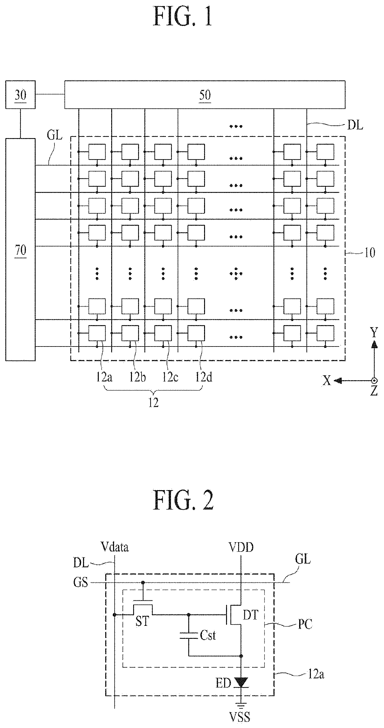
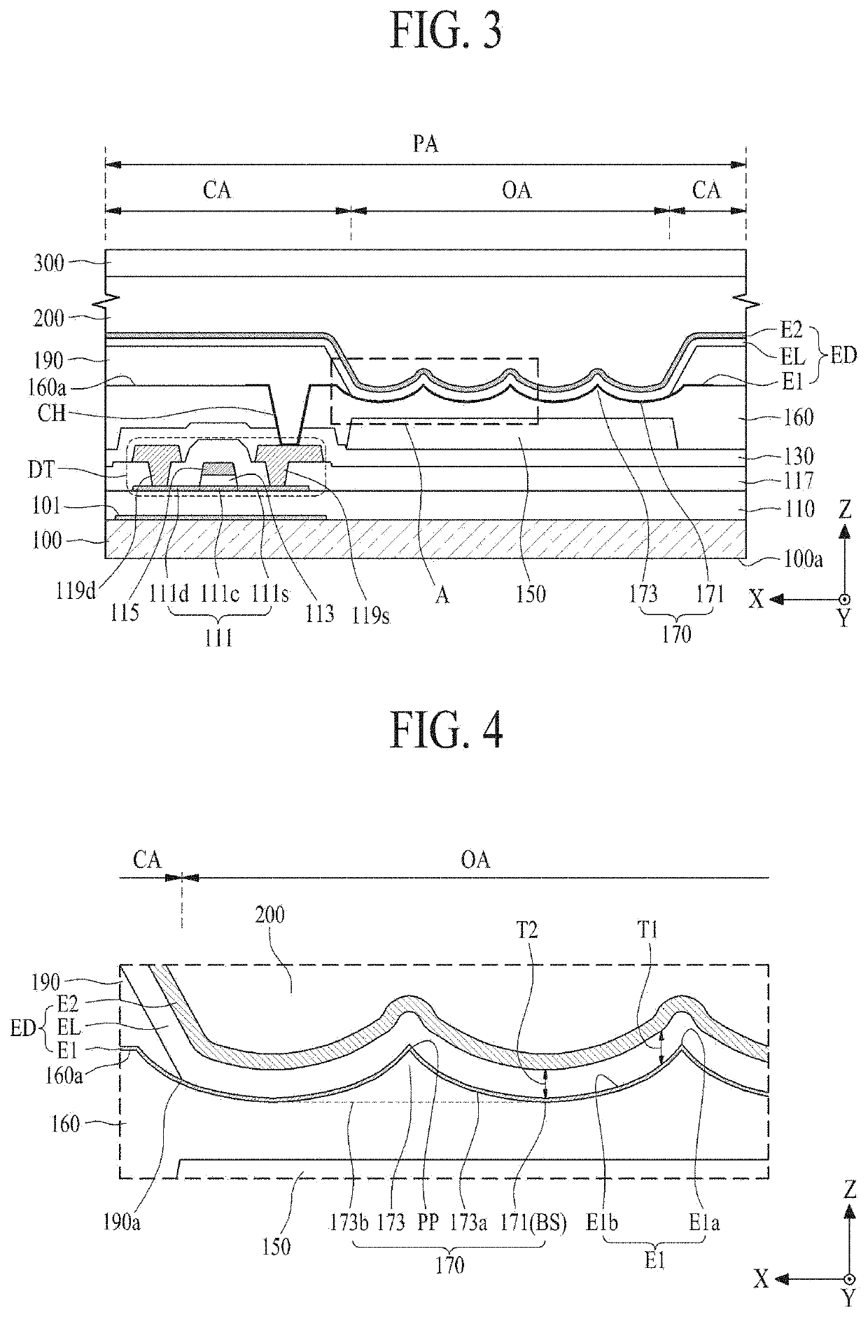
[0124]The wavelength conversion layer 150 includes a color filter that transmits only wavelengths of a color which is set for the pixel out of light emitted from the light emitting element ED to the substrate 100. For example, the wavelength conversion layer 150 may transmit only light with wavelengths of red, green, or blue. In the light emitting display device according to the present disclosure, when one unit pixel includes first to third pixels adjacent to each other, the wavelength conversion layer provided in the first pixel may include a red color filter, the wavelength conversion layer provided in the second pixel may include a green color filter, and the wavelength conversion layer provided in the third pixel may include a blue color filter. In addition, in the light emitting display device according to the present disclosure, one unit pixel may further include a white pixel in which a wavelength conversion layer is not formed.
second embodiment
[0125]The wavelength conversion layer 150 may include quantum dots having a size capable of re-emitting light according to light emitted from the light emitting element ED to the substrate 100 and discharging light of a color which is set for the pixel. In this case, the quantum dots may be selected from CdS, CdSe, CdTe, CdZnSeS, ZnS, ZnSe, GaAs, GaP, GaAs—P, Ga—Sb, InAs, InP, InSb, AlAs, AlP, and AlSb. For example, the wavelength conversion layer of the first pixel may include quantum dots of CdSe or InP, the wavelength conversion layer of the second pixel may include quantum dots of CdZnSeS, and the wavelength conversion layer of the third pixel may include quantum dots of ZnSe. In this way, the light emitting display device in which the wavelength conversion layer 150 includes quantum dots can realize high color reproducibility.
third embodiment
[0126]The wavelength conversion layer 150 may include a color filter including quantum dots.
[0127]The light emitting display device according to the present disclosure may further include a bank layer 190 and an encapsulation layer 200.
[0128]The bank layer 190 serves to define the opening area OA in the pixel area PA and is provided over an edge of the first electrode E1 and the overcoating layer 160. The bank layer 190 may be formed of an organic material such as a benzocyclobutene (BCB)-based resin, an acryl-based resin, or a polyimide resin. Alternatively, the bank layer 190 may be formed of a photosensitive material including a black pigment. In this case, the bank layer 190 also serves as a light blocking member between neighboring pixels.
[0129]The bank layer 190 according to an embodiment is formed over a flat surface 160a of the overcoating layer 160 to cover (or to overlay) the edge of the first electrode E1 extending over the circuit area CA of the pixel area PA.
[0130]The ...
PUM
Abstract
Disclosed is a light emitting display device that can enhance light extraction efficiency of light which is emitted from a light emitting element. The light emitting display device includes: an uneven portion that is provided on a substrate and includes a plurality of concave portions separated from each other and protruding portions between the plurality of concave portions; and a light emitting element that is provided on the uneven portion. Each protruding portion includes a vertex portion that is provided between three neighboring concave portions and a connection portion that is connected to two neighboring vertex portions between two neighboring concave portions and has a height less than that of the vertex portions.
Description
CROSS-REFERENCE TO RELATED APPLICATIONS[0001]This application claims the benefit of and priority to Korean Patent Application No. 10-2018-0103000, filed on Aug. 30, 2018, which is hereby incorporated by reference in its entirety as if fully set forth herein.BACKGROUNDTechnical Field[0002]The present disclosure relates to a light emitting display device.Description of the Related Art[0003]Since a light emitting display device has a high response speed and low power consumption and spontaneously emits light without using a particular light source unlike a liquid crystal display device, the light emitting display device does not cause a problem in a viewing angle and thus attracts attention as a next-generation flat panel display device.[0004]A light emitting display device displays an image by emission of light from light emitting elements including a light emitting layer interposed between two electrodes. In this case, light generated by emission of light from the light emitting elem...
Claims
Application Information
Patent Timeline
Application Date:The date an application was filed.
Publication Date:The date a patent or application was officially published.
First Publication Date:The earliest publication date of a patent with the same application number.
Issue Date:Publication date of the patent grant document.
PCT Entry Date:The Entry date of PCT National Phase.
Estimated Expiry Date:The statutory expiry date of a patent right according to the Patent Law, and it is the longest term of protection that the patent right can achieve without the termination of the patent right due to other reasons(Term extension factor has been taken into account ).
Invalid Date:Actual expiry date is based on effective date or publication date of legal transaction data of invalid patent.

