High light extraction efficiency (LEE) light emitting diode (LED)

Active Publication Date: 2019-08-01
PENN STATE RES FOUND
View PDF8 Cites 0 Cited by
  • Summary
  • Abstract
  • Description
  • Claims
  • Application Information

AI Technical Summary

Benefits of technology

[0014]In another embodiment in accordance with the present invention, a high-light-extraction efficiency light-emitting diode has a substrate with a first surface, an opposing second surface, and a reflection layer disposed on the first surface of the substrate. A light-emitting diode structure is arranged on the second surface of the substrate. The light-emitting diode structure includes a first semiconducting layer, an active layer, a second semiconducting layer and an overlayer disposed consecutively on the second surface. The overlayer has a plurality of protruding asymmetric micro-structured elements. To increase the light extraction efficiency, at least a portion of a surface of each micro-structured element of the overlayer is disposed at an obtuse angle with respect to the second semiconducting layer when measured from within the respective micro-stru

Problems solved by technology

Currently, concern about a global energy shortage has been raised again, and energy conservation has become an important issue.
Howeve

Method used


Image

  • High light extraction efficiency (LEE) light emitting diode (LED)
  • High light extraction efficiency (LEE) light emitting diode (LED)
  • High light extraction efficiency (LEE) light emitting diode (LED)

Examples


Example

[0034]Reference will now be made in detail to the embodiments of the present invention, an example of which is illustrated in the accompanying drawings. Wherever possible, the same reference numbers are used throughout the drawings and refer to the same or like parts.

[0035]Furthermore, it is required that the present invention is understood, not simply by the actual terms used, but by the meaning of each term laying within. Additional advantages, objects, and features of the invention will be set forth in part in the description that follows and in part will become apparent to those having ordinary skill in the art upon examination of the following or may be learned from practice of the invention. The objectives and other advantages of the invention may be realized and attained by the structure particularly pointed out in the written description and claims hereof as well as the appended drawings.

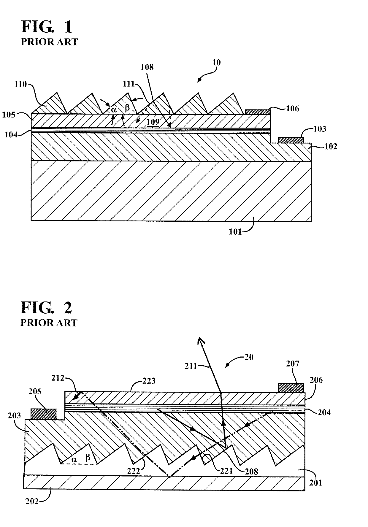
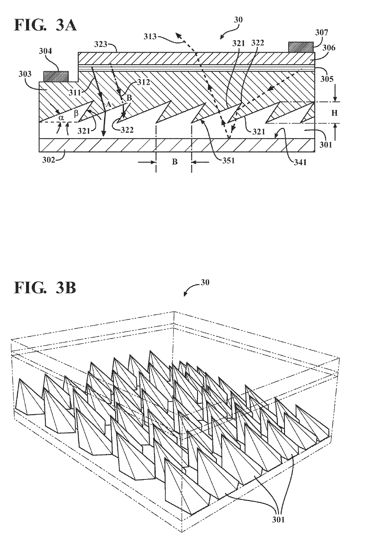
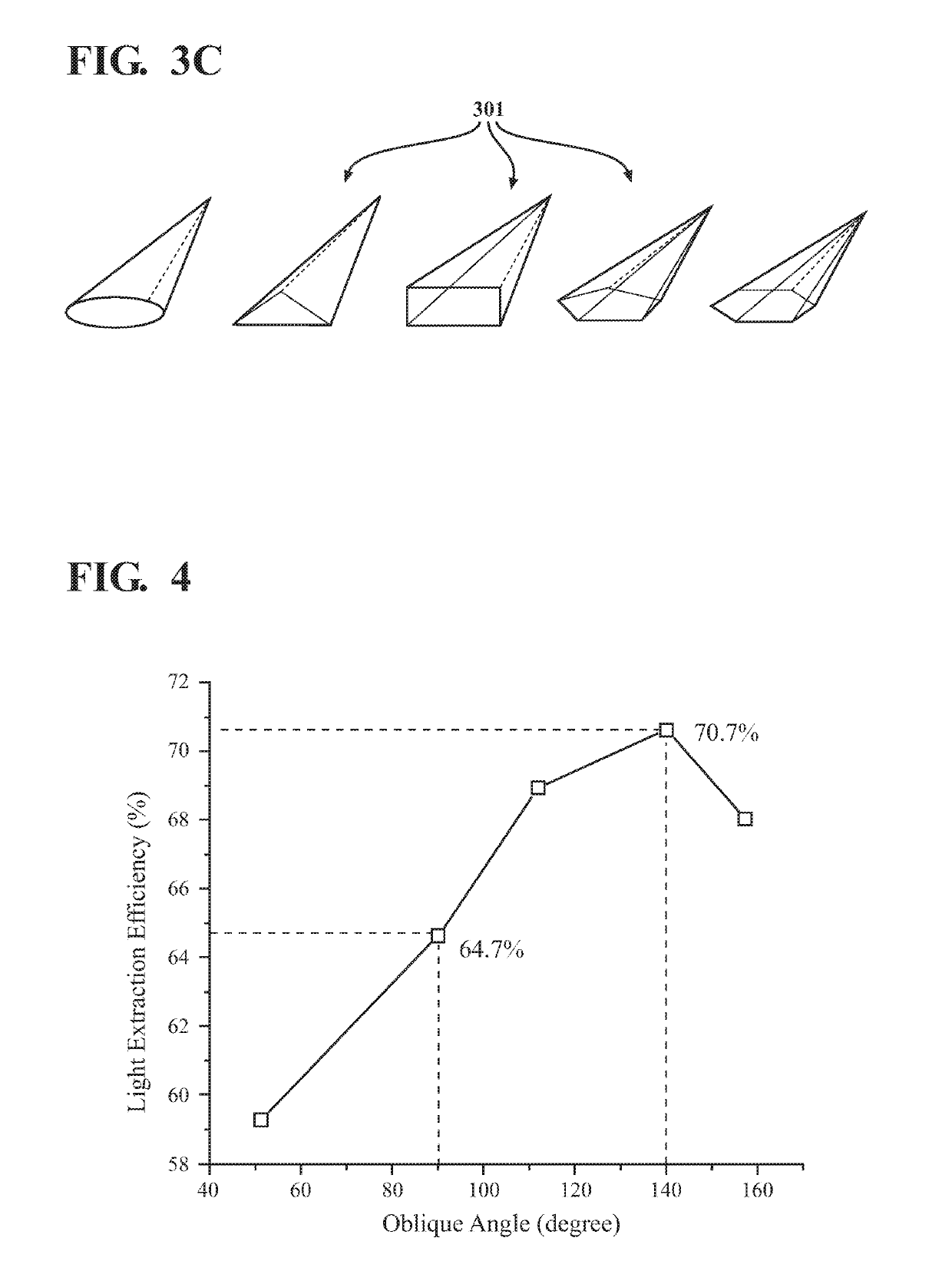
[0036]To overcome the limitations of the prior art micro-structured substrate, one embod...


PUM


Abstract

A light-emitting diode, comprising a substrate that has a first surface and an opposing second surface. A reflection layer is disposed on the first surface of the substrate and a light-emitting diode structure is arranged on the second surface of the substrate. The light-emitting diode structure includes a first semiconducting layer, an active layer and a second semiconducting layer disposed consecutively on the second surface. A plurality of protruding asymmetric micro-structured elements define at least a part of the second surface of the substrate such that at least a portion of a surface of each micro-structured element is disposed at an obtuse angle to the first surface of the substrate when measured from within the respective micro-structured element. The first semiconducting layer and the second semiconducting layer respectively have a first electrode and a second electrode.

Description

CROSS-REFERENCE TO RELATED APPLICATIONS[0001]This application claims priority to U.S. Provisional Application No. 62 / 379,888, filed on Aug. 26, 2016.FIELD OF THE INVENTION[0002]The present invention relates in general to Light-Emitting Diodes (LEDs) and, more particularly, to a design and method for a high light-extraction efficiency (LEE) LED.BACKGROUND OF THE INVENTION[0003]Light-emitting diodes (LED or LEDs) are solid-state devices that convert electric energy to light, and generally comprise one or more active layers of semiconductor material sandwiched between oppositely doped layers. When a voltage is applied across the doped layers, holes and electrons are injected into the active layer where they recombine to generate light. Light is emitted from the active layer and from all surfaces of the LED.[0004]Generally, an existing LED has been widely used as a backlight unit for a liquid crystal display device used in mobile phones, televisions (TVs), Personal Digital Assistants (P...

Claims


Application Information

Patent Timeline
IPC IPC(8): H01L33/22H01L33/06H01L33/30H01L33/32H01L33/60
CPCH01L33/22H01L33/06H01L33/305H01L33/325H01L33/60H01L33/20H01L33/0008H01L33/007H01L33/46H01L33/0093
Inventor YIN, SHIZHUOCHEN, CHANG-JIANGCHAO, JU-HUNGZHU, WENBIN
Owner PENN STATE RES FOUND
Why Eureka
Try Eureka